Semiconductor memory device capable of controlling drivability of overdriver

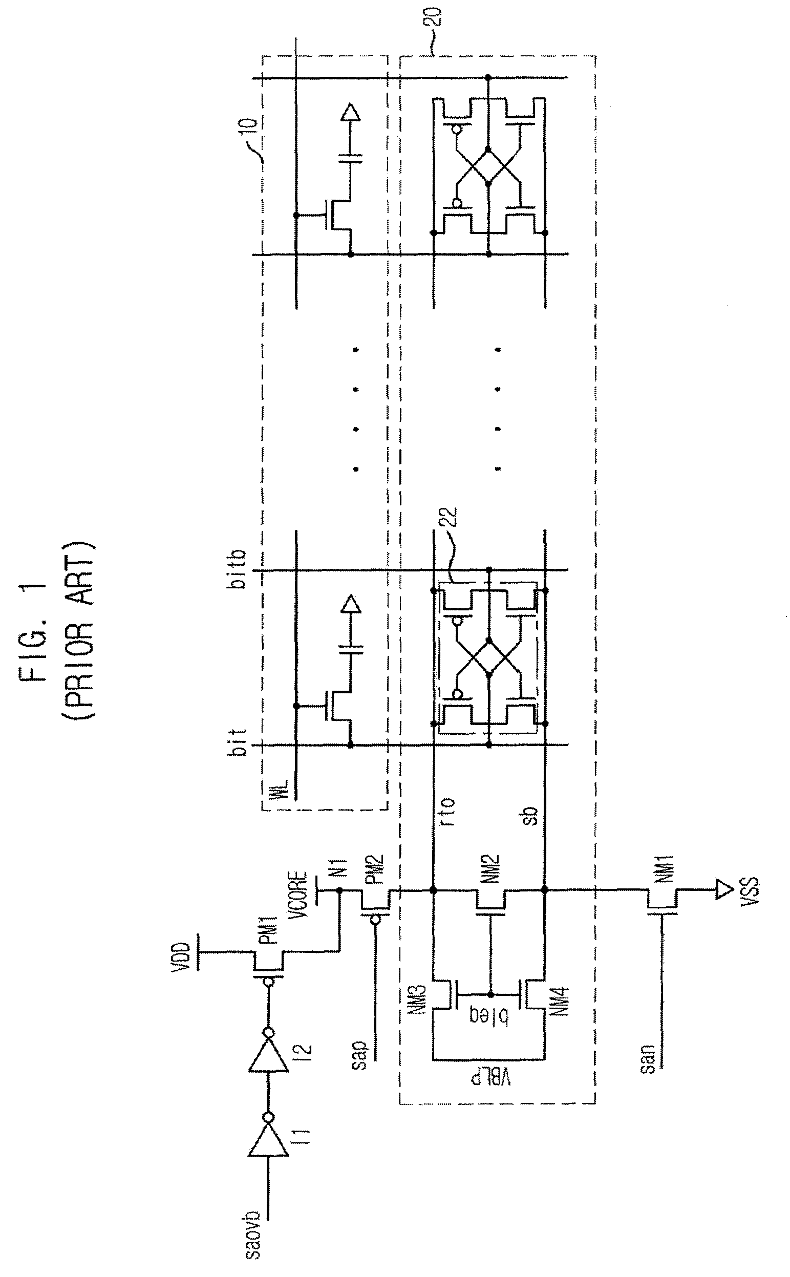
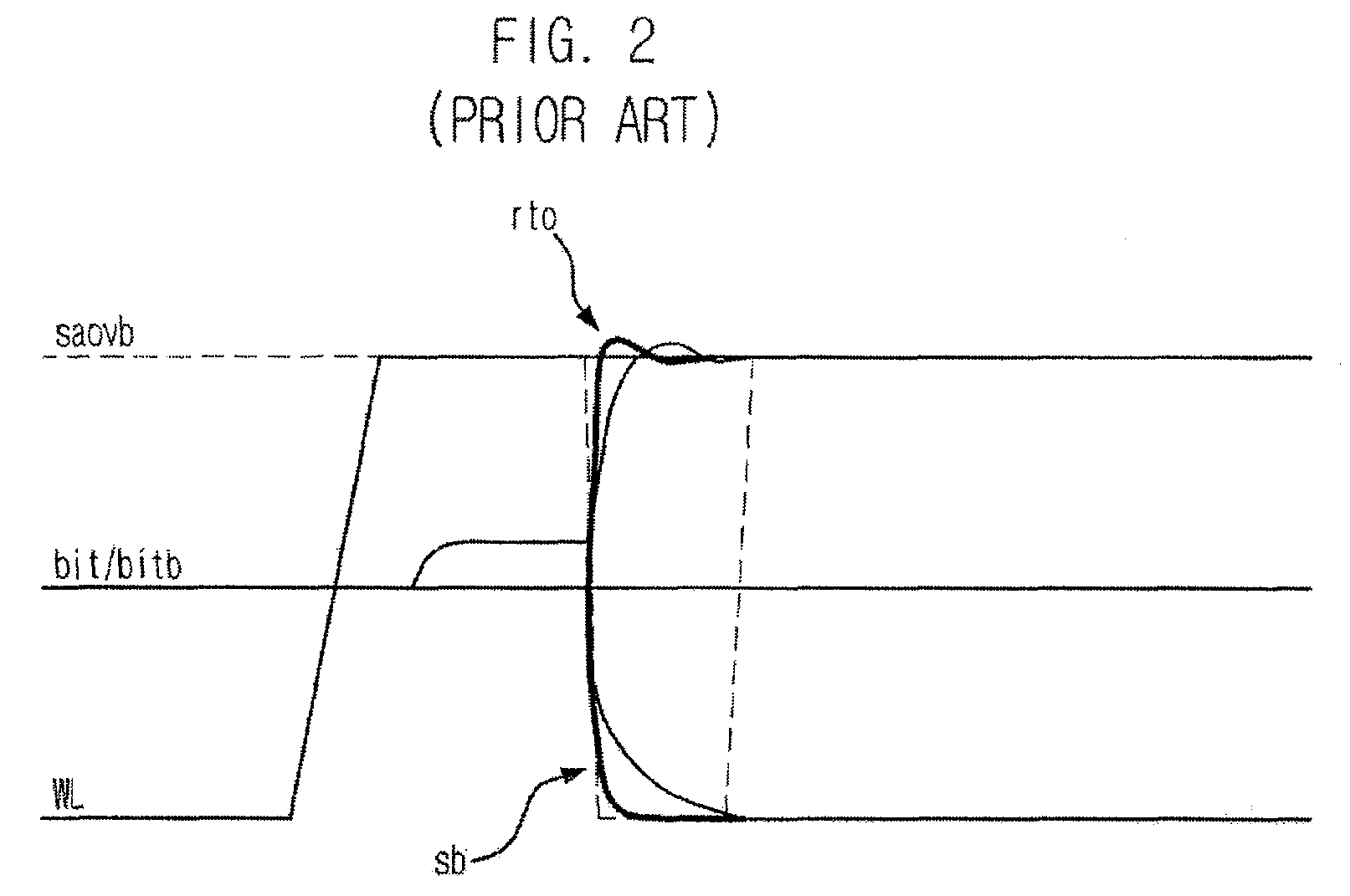
a memory device and memory technology, applied in static storage, digital storage, instruments, etc., can solve the problems of long time-consuming method, difficult to instantly supply a sufficient amount of current, and rise in the level of normal voltage vcores

Inactive Publication Date: 2008-04-22
SK HYNIX INC
View PDF6 Cites 16 Cited by
  • Summary
  • Abstract
  • Description
  • Claims
  • Application Information

AI Technical Summary

Problems solved by technology

However, with the tendency of the low driving voltage for the low power consumption, it is difficult to instantly supply a sufficient amount of current.
On the contrary, if the drivability of the overdriver is high, the level of the normal voltage VCORE rises much higher than a desired level, thereby causing noise.
However, this method requires a long time.

Method used


Image

  • Semiconductor memory device capable of controlling drivability of overdriver
  • Semiconductor memory device capable of controlling drivability of overdriver
  • Semiconductor memory device capable of controlling drivability of overdriver

Examples


first embodiment

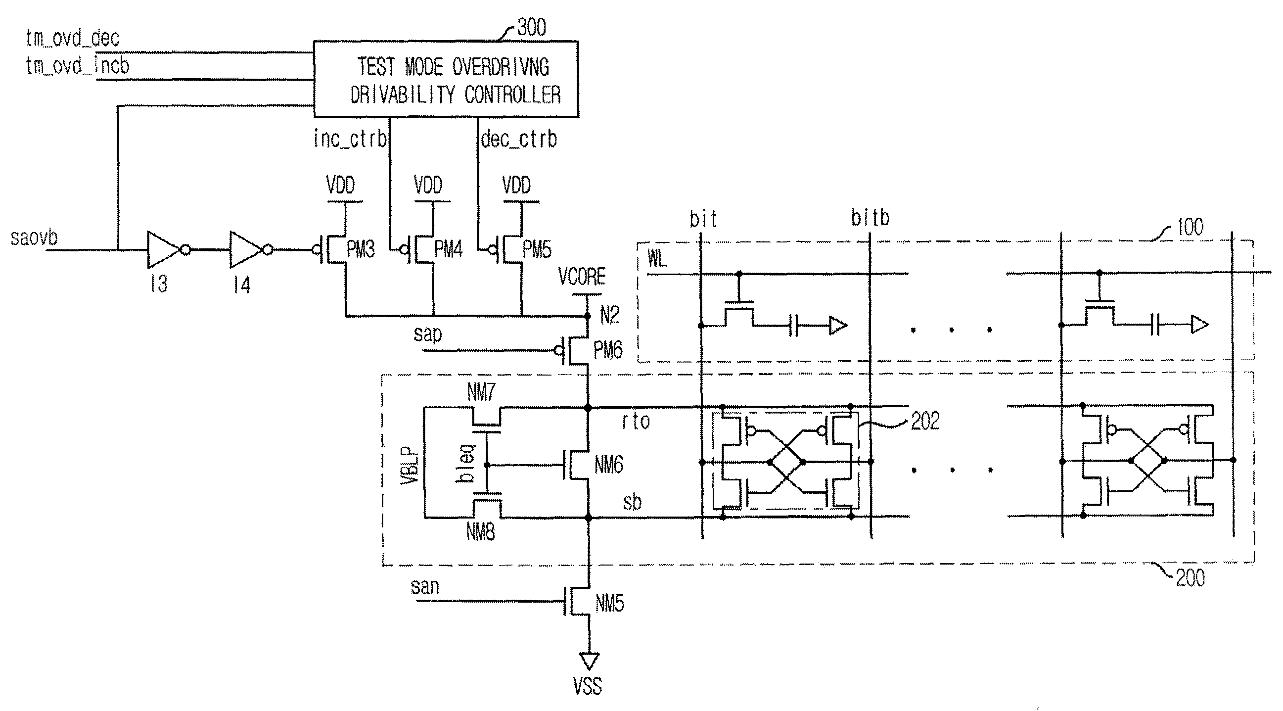
[0030]FIG. 4 is a circuit diagram of the test-mode overdriving drivability controller 300 in accordance with the present invention.

[0031]Referring to FIG. 4, the test-mode overdriving drivability controller 300 includes NOR gates NR1 and NR2 and inverters I5 and I6. The NOR gate NR1 receives the overdriving signal saovb and the test-mode drivability decreasing signal tm_ovd_dec, and the NOR gate NR1 receives the overdriving signal saovb and the test-mode drivability increasing signal tm_ovd_incb. The inverter I5 inverts an output signal of the NOR gate NR1 to generate a drivability decreasing signal dec_ctrb for controlling the overdriver PM4. Also, the inverter I6 inverts an output signal of the NOR gate NR2 to generate a drivability increasing signal inc_ctrb for controlling the overdriver PM5.

[0032]Hereinafter, an operation of the test-mode overdriving drivability controller 300 will be described in detail.

[0033]When the overdriving signal saovd is in an inactive state before the...

second embodiment

[0035]FIG. 5 is a circuit diagram of the test-mode overdriving drivability controller 300 in accordance with the present invention.

[0036]Referring to FIG. 5, the test-mode overdriving drivability controller 300 includes transfer gates 322 and 324, latches 326 and 328, and PMOS transistors PM7 and PM8.

[0037]The transfer gate 322 transfers the overdriving signal saovb in response to the test-mode drivability decreasing signal tm_ovd_dec and the transfer gate 324 transfers the overdriving signal saovb in response to the test-mode drivability increasing signal tm_ovd_incb. The latch 326 latches an output signal of the transfer gate 322 through an inverter I7 and generates the drivability decreasing signal dec_ctrb, and the latch 328 latches an output signal of the transfer gate 344 through an inverter I8 and generates the drivability increasing signal inc_ctrb.

[0038]The PMOS transistors PM7 and PM 8 are provided at output nodes of the transfer gates 322 and 324, respectively. The PMOS t...


PUM


Abstract

A semiconductor memory device capable of controlling a drivability of an overdriver is provided. The semiconductor memory device includes: a first power supply for supplying a normal driving voltage; a memory cell array block; a bit line sense amplifier block for sensing and amplifying voltage difference between bit line pair of the memory cell array block; a first driver for driving a power supply line of the bit line sense amplifier block to a voltage of a node connected with the first power supply in response to a driving control signal; a plurality of second drivers for driving the node to an overdriving voltage higher than the normal driving voltage; and an overdriving drivability controller for selectively activating the second drivers in response to a test-mode drivability control signal inputted during an activation period of an overdriving signal.

Description

FIELD OF INVENTION [0001]The present invention relates to a semiconductor design technology; and, more particularly, to a semiconductor memory device capable of controlling a drivability of an overdriver.DESCRIPTION OF PRIOR ART[0002]Since a low driving voltage is used for the low power consumption, a memory device including a DRAM employs an overdriving structure to help an operation of a sense amplifier.[0003]In general, if word lines are activated by row addresses, data stored in a plurality of memory cells connected to word lines are transferred to bit lines and a bit line sense amplifier (BLSA) sense and amplify voltage difference between bit line pair.[0004]During the above operation, thousands of bit line sense amplifiers are operated at the same time. Thus, a driving time of the bit line sense amplifier is determined by an amount of current supplied thereto. However, with the tendency of the low driving voltage for the low power consumption, it is difficult to instantly supp...

Claims


Application Information

Patent Timeline
Patent Type & Authority Patents(United States)
IPC IPC(8): G11C7/00G11C8/00G11C5/14G11C7/02G11C7/08G11C29/14
CPCG11C7/08G11C29/14G11C2207/065A43D35/00
Inventor JANG, JI-EUN
Owner SK HYNIX INC
Why Eureka
Try Eureka