Multi-level semiconductor module and method for fabricating the same

a semiconductor module and multi-level technology, applied in the direction of semiconductor devices, semiconductor/solid-state device details, electrical devices, etc., can solve the problems of partial failure of packaging, semiconductor module warp, and the like, and achieve the effect of reducing the thickness of semiconductor chips, high yield, and increasing the number of levels of such stacked semiconductor chips

Active Publication Date: 2008-04-29
PANASONIC SEMICON SOLUTIONS CO LTD
View PDF13 Cites 143 Cited by
  • Summary
  • Abstract
  • Description
  • Claims
  • Application Information

AI Technical Summary

Benefits of technology

[0010]In recent years, techniques for reducing the thickness of semiconductor chips by polishing and techniques for mounting the thin semiconductor chips on boards with high yields have been developed, so that the number of levels of such stacked semiconductor chips has been further increasing. In addition, in a semiconductor memory, for example, as the memory capacity increases, the chip area increases. If a module is formed by stacking large semiconductor chips in multiple levels, the problem of a warp of the module arises. The degree of warp of the module increases as the thickness of a printed board decreases. Accordingly, to stack printed boards on which semiconductor chips are mounted and interlayer members in multiple levels, it is important to suppress the occurrence of a warp.

Problems solved by technology

If a module is formed by stacking large semiconductor chips in multiple levels, the problem of a warp of the module arises.
Accordingly, if a warp occurs at room temperature or is caused by heating during bonding, a semiconductor module cannot be mounted on the mother board or the warp causes a partial failure in packaging.
That is, a semiconductor module can be defective in packaging though it is non-defective in its electric characteristics.

Method used


Image

  • Multi-level semiconductor module and method for fabricating the same
  • Multi-level semiconductor module and method for fabricating the same
  • Multi-level semiconductor module and method for fabricating the same

Examples


embodiment 1

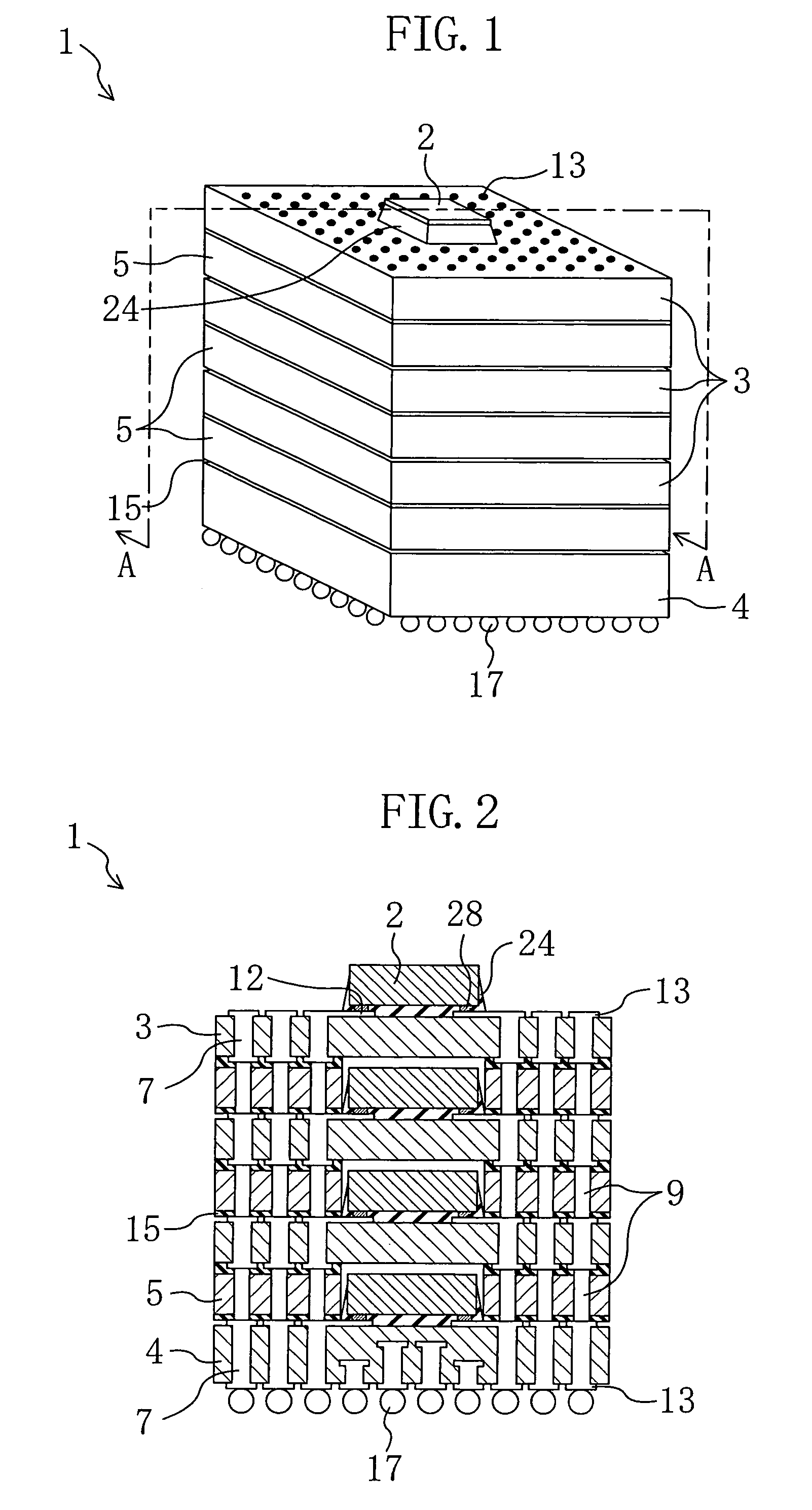
[0050]A multi-level semiconductor module according to a first embodiment of the present invention will be described with reference to FIGS. 1, 2, 3A through 3C and 4A through 4C.

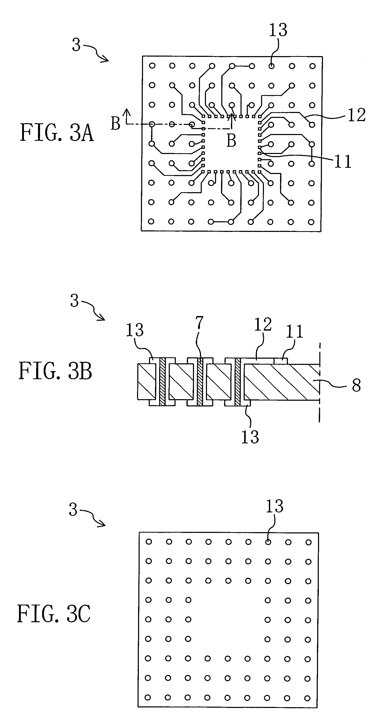
[0051]FIG. 1 is a perspective view schematically illustrating an overall structure of a semiconductor module 1 according to this embodiment of the present invention. FIG. 2 is a cross-sectional view taken along the line A-A in FIG. 1. FIGS. 3A through 3C are a plan view schematically illustrating the shape of a resin board of this embodiment, a partial cross-sectional view taken along the line B-B, and a plan view schematically illustrating the back face of the resin board, respectively. FIGS. 4A through 4C are schematic plan views and a partial cross-sectional view for explaining the shape of a sheet member. In these drawings, the thicknesses, lengths and shapes, for example, of parts of the semiconductor module are selected so as to be easily shown, and therefore are different from those of actual parts. T...

embodiment 2

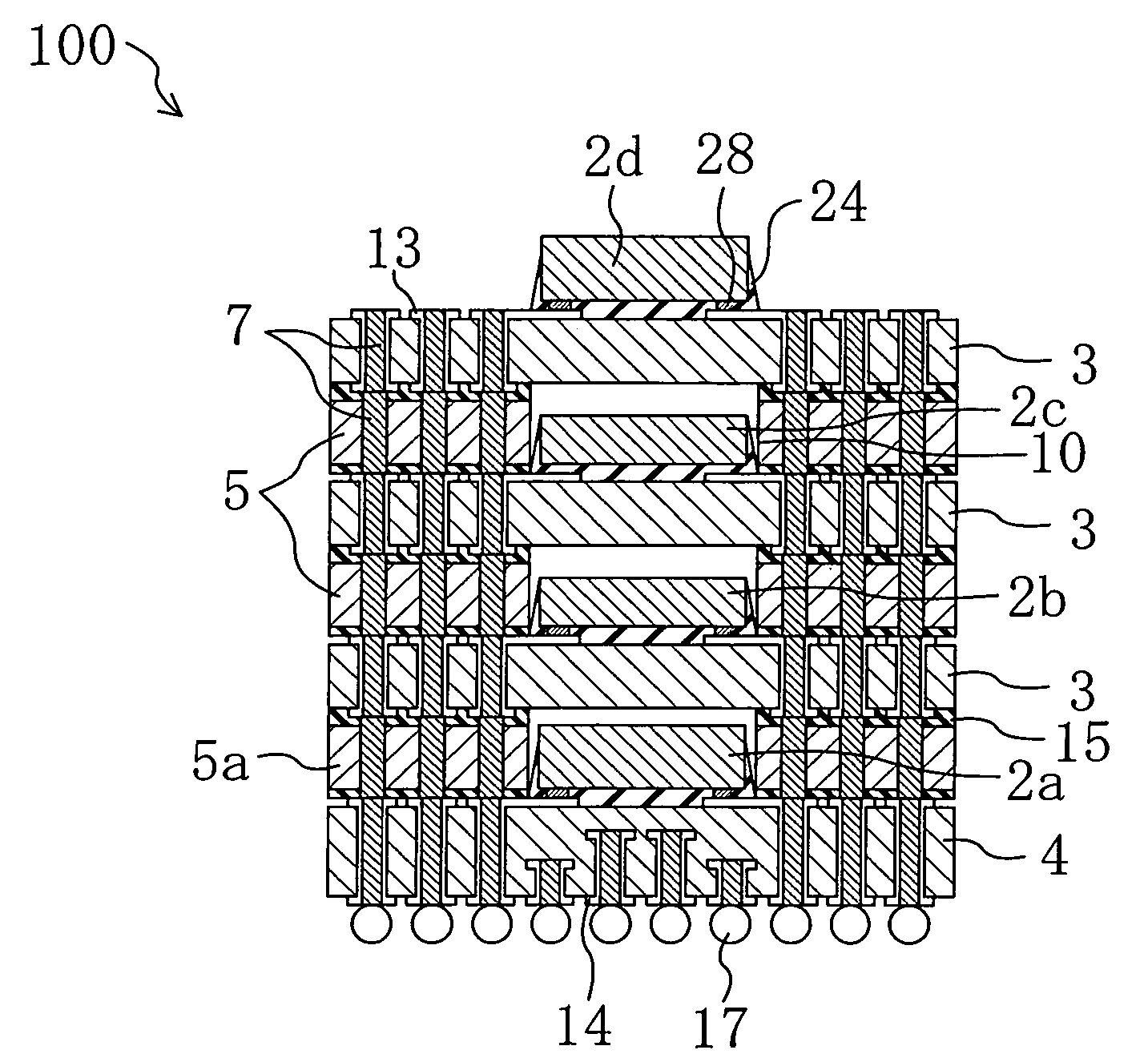
[0089]Hereinafter, a multi-level semiconductor module 100 according to a second embodiment of the present invention will be described with reference to FIG. 9.

[0090]The semiconductor module 100 of this embodiment has a characteristic in which a semiconductor chip 2d mounted on a first resin board 3 located at the top and a semiconductor chip 2a mounted on a second resin board 4 located at the bottom are thicker than semiconductor chips 2b and 2c mounted on the other first resin boards 3. Accordingly, the lowest-level sheet member 5a is thicker than the other sheet members 5 in the semiconductor module 100 of this embodiment. With respect to the other aspects, the semiconductor module 100 of this embodiment is the same as the semiconductor module 1 of the first embodiment, and description thereof will be omitted. Likewise, in the following embodiments, only aspects different from those of the preceding embodiments will be described.

[0091]With the structure of the semiconductor module...

embodiment 3

[0093]A multi-level semiconductor module 110 according to a third embodiment of the present invention will be described with reference to FIG. 10.

[0094]FIG. 10 is a cross-sectional view illustrating a semiconductor module of this embodiment. As illustrated in FIG. 10, the semiconductor module 110 of this embodiment has a characteristic in which a rigid plate 22 having the same area as that of the first resin boards 3 is attached to the top of the semiconductor module 1 of the first embodiment. Specifically, in the semiconductor module 110 of this embodiment, a base 23 having an opening capable of accommodating a semiconductor chip 2 and a rigid plate 22 having the same shape as that of the first resin boards 3 and a thermal conductivity higher than that of the first resin boards 3 are further provided on the first resin board 3 located at the top, in addition to the components of the semiconductor module 1 of the first embodiment. To bond the base 23 and the rigid plate 22, these ba...


PUM


Abstract

A semiconductor module is formed by alternately stacking resin boards 3 on which semiconductor chips 2 are mounted and sheet members having openings larger than the semiconductor chips 2 and bonded to the resin boards 3. The resin board 4 located at the bottom out of the resin boards 3 is thicker than the other resin boards 3.

Description

CROSS-REFERENCE TO RELATED APPLICATION[0001]This application claims priority under 35 U.S.C. §119(a) on Patent Application No. 2004-364586 filed in Japan on Dec. 16, 2004, the entire contents of which are hereby incorporated by reference.BACKGROUND OF THE INVENTION[0002]1. Field of the Invention[0003]The present invention relates to three-dimensional multi-level semiconductor modules formed by alternately stacking sheet members and resin boards on which semiconductor chips are mounted and also relates to methods for fabricating the modules.[0004]2. Description of the Related Art[0005]With demands for size reduction and performance improvement of various electronic devices such as cellular phones and digital cameras, multi-level semiconductor modules formed by stacking and uniting a plurality of electronic components, especially semiconductor chips, have been proposed.[0006]Methods for easily manufacturing such multi-level semiconductor modules at low cost have been proposed to date....

Claims


Application Information

Patent Timeline
Patent Type & Authority Patents(United States)
IPC IPC(8): H01L23/02
CPCH01L21/486H01L21/563H01L23/49816H01L25/105H01L2224/16225H01L2224/73203H01L2224/73204H01L2924/01078H01L2924/15173H01L2924/15311H01L2924/3011H01L2924/3511H01L2224/32225H01L2924/00012H01L2225/1023H01L2225/107H01L2225/1094H01L2924/00H01L2924/1627H01L23/12
Inventor KAWABATA, TAKESHISATOU, MOTOAKIFUKUDA, TOSHIYUKITSUDA, TOSHIONOBORI, KAZUHIRONAKATANI, SEIICHI
Owner PANASONIC SEMICON SOLUTIONS CO LTD
Why Eureka
Try Eureka