Switched capacitor amplifier with higher gain and improved closed-loop gain accuracy

a switched capacitor and amplifier technology, applied in the field of amplifier circuits, can solve the problems of introducing finite gain errors, low gain of cmos switched amplifiers, and typical cmos differential amplifiers with open-loop gain that even approaches infinity, and achieves the effect of small gain and high gain

Active Publication Date: 2008-04-29
MICRON TECH INC
View PDF60 Cites 12 Cited by
  • Summary
  • Abstract
  • Description
  • Claims
  • Application Information

AI Technical Summary

Problems solved by technology

However, CMOS amplifiers have a relatively low gain because of the low gain inherent in CMOS devices.
The low gain of CMOS switched amplifiers introduce finite gain error when the gain of the amplifier is assumed to be the ratio of the capacitance of an input capacitance to the capacitance of a feedback capacitor.
However, a typical CMOS differential amplifier does not have an open-loop gain that even approaches infinity.
However, since CMOS amplifiers invariably do not have high open-loop gain, equation (2) does not provide an accurate result.
The error, which is the difference in gain, is caused by the low open-loop gain of the CMOS amplifier.
However, it is fairly impractical to fabricate a CMOS amplifier with a precisely controlled open-loop gain since the gain can vary with process variations.
However, all of these approaches impose limitations or costs on switched capacitance CMOS amplifiers using these approaches.
For example, some approaches result in the use of greatly increased surface area on a die, and other approaches provided somewhat limited performance.

Method used


Image

  • Switched capacitor amplifier with higher gain and improved closed-loop gain accuracy
  • Switched capacitor amplifier with higher gain and improved closed-loop gain accuracy
  • Switched capacitor amplifier with higher gain and improved closed-loop gain accuracy

Examples


Embodiment Construction

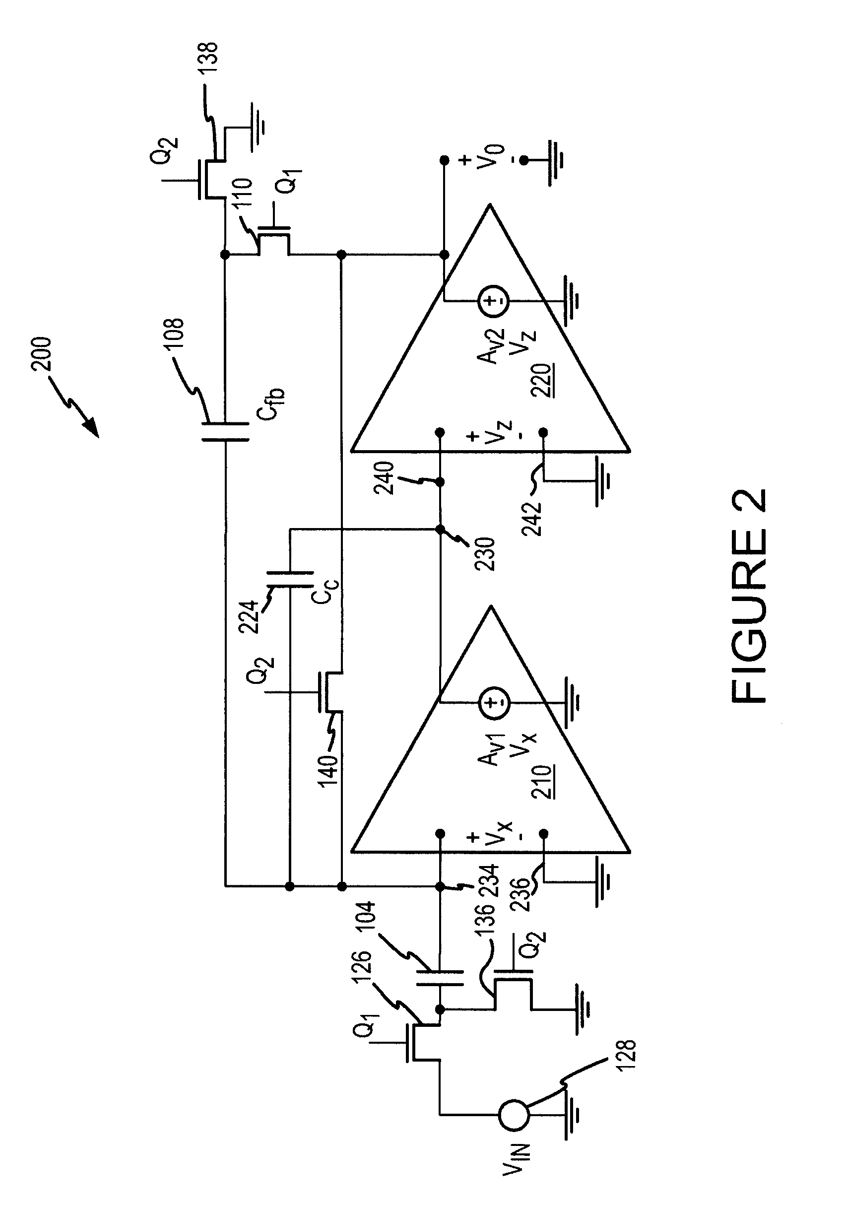
[0021]A switched capacitance CMOS amplifier 200 according to one example of the invention is shown in FIG. 2. The amplifier 200 uses a first CMOS amplifier 210, a second CMOS amplifier 220, and the same components that were used externally to the amplifiers 210, 220 that were used externally of the amplifier 112 in the amplifier 100 shown in FIG. 1. In addition, the first CMOS amplifier 210 includes a capacitor 224 having a capacitance of Cc connected between its output 230 and a non-inverting input 234. An inverting input of the 236 of the amplifier 210 is connected to ground. In operation, the capacitor 224 provides the amplifier 210 with positive feedback, thereby greatly increasing its gain.

[0022]The output 230 of the first CMOS amplifier 210 is connected to an inverting input 240 of the second CMOS amplifier 220. A non-inverting input 242 of the amplifier 220 is connected to ground. The amplifier 220, like typical CMOS amplifiers, has a relatively low gain. However, because of ...


PUM


Abstract

A switched capacitor CMOS amplifier uses a first stage non-inverting CMOS amplifier driving a second stage inverting CMOS amplifier. The first stage amplifier is provided with positive feedback to substantially increase the gain of the first stage amplifier. In the described examples, the positive feedback is provided either by connecting a capacitor from the output to the input of the first stage amplifier or by connecting a shunt transistor in parallel with an input transistor and driving the transistor from the output of the first stage amplifier. The substantially increased gain resulting from the positive feedback allows the gain of the switched capacitor amplifier to be set by the ratio of the capacitance of an input capacitor to the capacitance of a feedback capacitor. The amplifier also includes switching transistors for periodically discharging the input capacitor and the feedback capacitor.

Description

TECHNICAL FIELD[0001]This invention relates to amplifier circuits, and, more particularly, to a switched capacitor amplifier circuit that provides higher open-loop gain and improved closed-loop gain accuracy.BACKGROUND OF THE INVENTION[0002]Switched capacitor amplifiers are compatible with CMOS technology and consequently are therefore frequently used as analog building blocks in CMOS circuits. In general, the design methodology in CMOS amplifiers assumes the use of infinite gain and infinite bandwidth operational amplifiers. However, CMOS amplifiers have a relatively low gain because of the low gain inherent in CMOS devices. The maximum gain of a CMOS switched amplifier, i.e., open circuit gain, is approximately 25, and may be as low as 10. The low gain of CMOS switched amplifiers introduce finite gain error when the gain of the amplifier is assumed to be the ratio of the capacitance of an input capacitance to the capacitance of a feedback capacitor.[0003]FIG. 1 shows a switched ca...

Claims


Application Information

Patent Timeline
Patent Type & Authority Patents(United States)
IPC IPC(8): H03F1/02
CPCH03F1/38H03F3/005H03F3/45183H03F3/45475H03F2203/45514
Inventor FORBES, LEONARD
Owner MICRON TECH INC
Why Eureka
Try Eureka