Semiconductor memory device

a memory device and semiconductor technology, applied in the field of methods, can solve the problems of reducing the operating frequency and the need for an external command, and achieve the effect of high speed

Active Publication Date: 2008-04-29
SOCIONEXT INC
View PDF7 Cites 9 Cited by
  • Summary
  • Abstract
  • Description
  • Claims
  • Application Information

AI Technical Summary

Benefits of technology

[0018]In the above-described arrangement, the sources of the N-type transistors of the write circuit are connected to ground potential and the drains of the N-type transistors are connected to the bit lines, the connections being made without intermediation by a selector circuit. Also, only the single-stage N-type transistor circuit operates at the time of writing. The arrangement therefore ensures that the potential on the bit line can be pulled at a high speed at a voltage lower than a normal voltage, without increasing the word line activation period at the normal voltage, thus enabling low-voltage high-speed writing. Also, the need for an external command according to the operating voltage can be eliminated.
[0020]With this arrangement, the potential on the bit line is set to the negative potential at the time of writing, thereby enabling writing at a higher speed even at a low voltage lower than the normal voltage.
[0026]In this arrangement, the application of the forward bias enables writing to be performed at a higher speed.
[0027]As described above, the semiconductor memory device of the present invention can pull the potential on the bit line at a high speed at a voltage lower than a normal voltage, without increasing the word line activation period at the normal voltage, and thus has the advantage of performing high-speed writing even at such low voltage.

Problems solved by technology

However, if the word line WL activation period (pulse width) is increased to correspond to a lower voltage, there is a problem that the word line WL activation period is made to be longer than necessary at the normal voltage, causing reduction in operating frequency.
There is also a problem that a need arises for an external command according to the operating voltage.

Method used


Image

  • Semiconductor memory device
  • Semiconductor memory device
  • Semiconductor memory device

Examples


embodiment 1

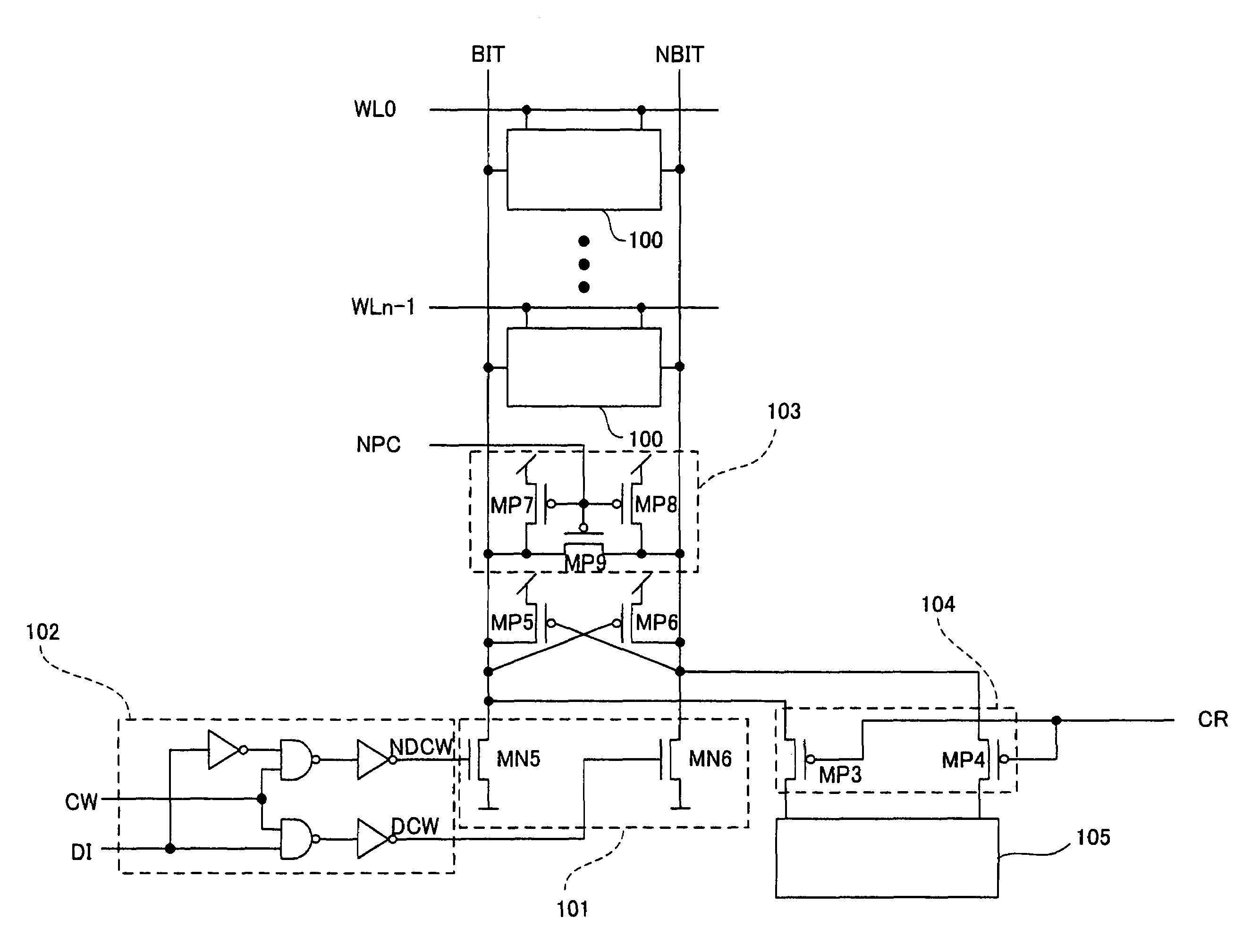
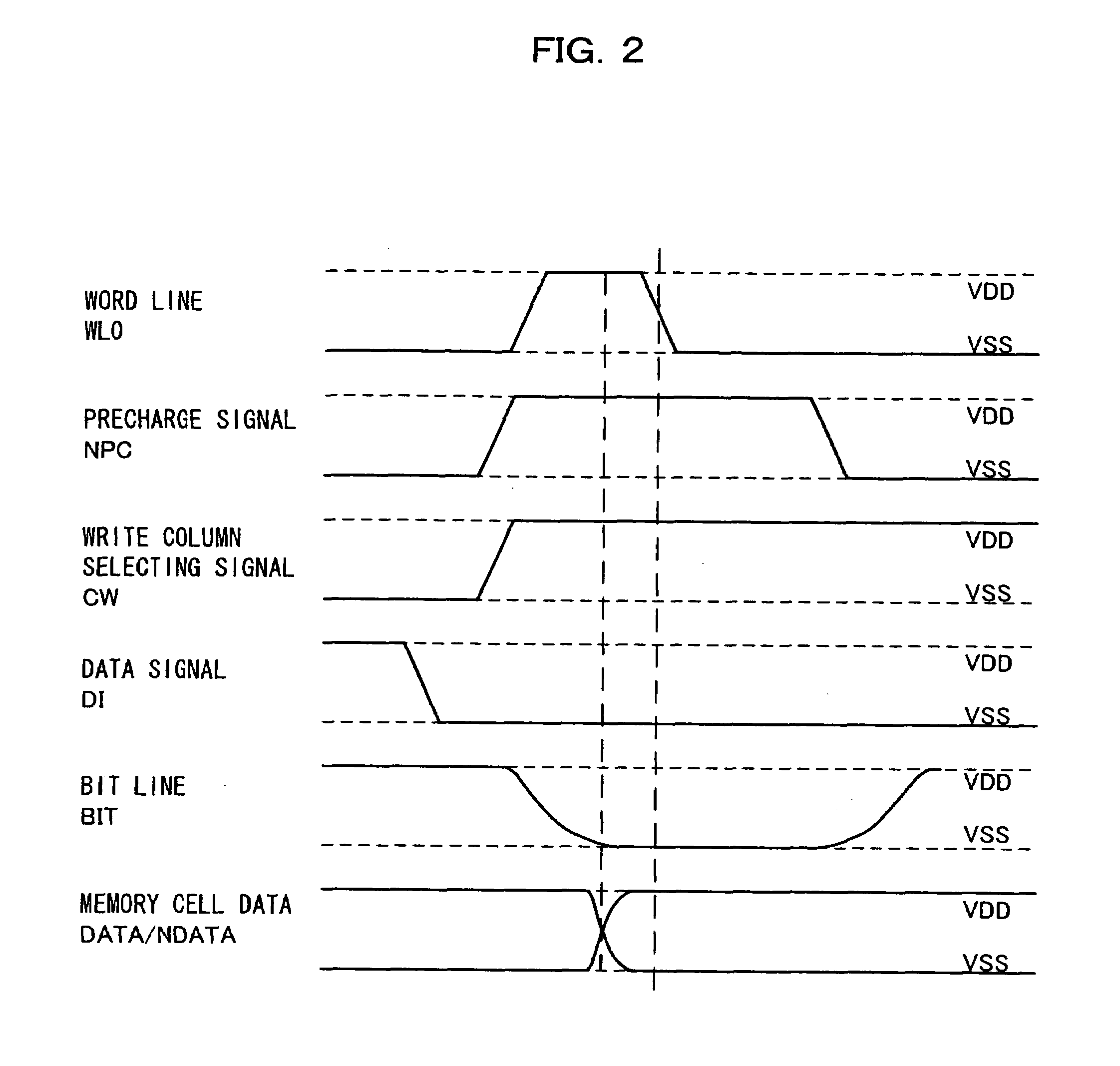
[0037]FIG. 1 is a diagram showing the configuration of a semiconductor memory device in Embodiment 1 of the present invention.

[0038]In Embodiment 1 of the present invention, a write circuit 101 and a column selecting and data input circuit 102 are provided in place of the write column selector 701 and the write circuit 702 in the background art. The same circuit for the memory cell 100 as that shown in FIG. 7 is also provided.

[0039]The write circuit 101 is constituted by two NMOS transistors MN5 and MN6. The sources of the transistors MN5 and MN6 are connected to VSS. The drain of the transistor MN5 is connected to the bit line BIT, while the drain of the N-type transistor MN6 is connected to the bit line NBIT.

[0040]In the column selecting and data input circuit 102, a logical product NDCW of inverted data of data DI to be written and the write column selecting signal CW is generated and a logical product DCW of the data DI to be written and the write column selecting signal CW is a...

embodiment 2

[0047]FIG. 3 is a diagram showing the configuration of a semiconductor memory device in Embodiment 2 of the present invention.

[0048]In the above-described configuration of Embodiment 1, the sources of the transistors MN5 and MN6 of the write circuit 101 are connected to VSS. In Embodiment 2 of the present invention, the sources of the transistors MN5 and MN6 are connected to a negative power supply circuit 401 set to a negative potential, and the bit line BIT or NBIT is set to the negative potential at the time of writing.

[0049]As shown in FIG. 4, the substrates of the four NMOS transistors, i.e., the two drive transistors MN1 and MN2 and the two transfer transistors MN3 and MN4, of the memory cells 100 in each column are respectively connected to potentials VSSB0n to VSSBn-1. Each of the substrate potentials VSSB0n to VSSBn-1 is set lower than VSS to apply a back bias to the four NMOS transistors MN1, MN2, MN3, and MN4.

[0050]The operation based on the above-described configuration ...


PUM


Abstract

A semiconductor memory device capable of performing a high-speed write operation at lower voltage without increasing the word line activation period at normal voltage. The memory device has a write circuit including two NMOS transistors respectively having sources connected to ground potential. One of the transistors has a drain connected to one of a pair of bit lines, and the other transistor has a drain connected to the other bit line. The memory device also has a column selecting and data input circuit which generates a logical product of inverted data of data to be written and a write column selecting signal, inputs the logical product to the gate of the one transistor, generates a logical product of the data to be written and the write column selecting signal, and inputs the logical product to the gate of the other transistor.

Description

FIELD OF THE INVENTION[0001]The present invention relates to a semiconductor memory device, and more particularly, to a method of writing in the semiconductor memory device.BACKGROUND OF THE INVENTION[0002]A static random-access memory (SRAM), which is one of conventional semiconductor devices, will be described with reference to a circuit diagram in FIG. 6.[0003]As shown in FIG. 6, memory cells 100 are disposed in an array and are each connected to a word line WL and to a pair of bit lines (BIT, NBIT).[0004]As shown in FIG. 7, the memory cell 100 has a total of six transistors, i.e., two PMOS transistors MP1 and MP2 provided as load transistors, two NMOS transistors MN1 and MN2 provided as drive transistors, and two NMOS transistors MN3 and MN4 provided as transfer transistors, whereby a memory cell of an SRAM is formed.[0005]That is, the gates of the two transfer transistors MN3 and MN4 are connected to the word lines WL, and the drains of the transfer transistors MN3 and MN4 are ...

Claims


Application Information

Patent Timeline
Patent Type & Authority Patents(United States)
IPC IPC(8): G11C11/00
CPCG11C7/1006G11C7/1078G11C7/1096G11C11/413
Inventor KANEHARA, HIDENARI
Owner SOCIONEXT INC
Why Eureka
Try Eureka