Level-shifting pass gate multiplexer

a multiplexer and gate technology, applied in the field of multiplexer circuits, can solve the problems of increasing circuit area, introducing circuit delays for select signals sa-sc, complicating circuit fabrication, etc., and achieves the effect of reducing circuit area, reducing gate delays, and reducing circuit delays

Active Publication Date: 2008-05-06
XILINX INC
View PDF7 Cites 26 Cited by
  • Summary
  • Abstract
  • Description
  • Claims
  • Application Information

AI Technical Summary

Benefits of technology

[0013]For some embodiments, the first and second multiplexers are organized as hierarchical levels of pass transistors, for example, where the pass transistors in the first level are organized in pairs and are coupled to receive the input signals, and the transistors in the second level are coupled between corresponding transistor pairs in the first level and output terminals in the second level. For one embodiment, the gates of the transistors in the first level are responsive to the low-voltage select signals, and the gates of the transistors in the second level are responsive to the high-voltage decoded select signals. By driving the pass gates in the second hierarchical level with high-voltage select signals, as opposed to low-voltage select signals, propagation delays across the pass gates are reduced. In addition, by utilizing decoded select signals to control the second hierarchical level, the third hierarchical level of previous MUX architectures may be eliminated, thereby reducing circuit area and reducing the number of gate delays.
[0014]For other embodiments, the first and second multiplexers are organized as hierarchical levels of pass transistors, for example, where the pass transistors in the first hierarchical level receive the input signals and are responsive to the low-voltage encoded select signals, and the transistors in the second hierarchical level are arranged in pairs and are responsive to the high-voltage decoded select signals. By driving the pass gates in the first hierarchical level with high-voltage select signals, as opposed to low-voltage select signals, propagation delays across the pass gates are reduced. In addition, by utilizing decoded select signals to control the first hierarchical level, the third hierarchical level of previous MUX architectures may be eliminated, thereby reducing circuit area and reducing the number of gate delays.
[0015]In addition, the output circuit restores the voltage levels of signals propagated through the multiplexer circuit to their maximum values, thereby ensuring that the output inverters trigger properly and also maintaining an acceptable drive strength for the output signals.
[0016]Further, the invention enables the use of multiplexers that include only N-channel transistors in the signal paths between the data input and output terminals, even at very low operating voltages. Power dissipation and leakage current are also lower than is normally achieved using traditional multiplexer circuits. Additionally, the layout area required to implement the resulting structures is less than is required for traditional CMOS implementations.

Problems solved by technology

However, this solution complicates the fabrication of the circuit, especially at very short gate lengths.
Unfortunately, using level-shifters for select signals SA-SC not only increases circuit area but also introduces circuit delays for select signals SA-SC.

Method used


Image

  • Level-shifting pass gate multiplexer
  • Level-shifting pass gate multiplexer
  • Level-shifting pass gate multiplexer

Examples


Embodiment Construction

[0028]In the following description, for purposes of explanation, specific nomenclature is set forth to provide a thorough understanding of the present invention. In other instances, well-known circuits and devices are shown in block diagram form to avoid obscuring the present invention unnecessarily. Further, the logic states of various signals described herein are exemplary and therefore may be reversed or otherwise modified as generally known in the art. Accordingly, the present invention is not to be construed as limited to specific examples described herein but rather includes within its scope all embodiments defined by the appended claims.

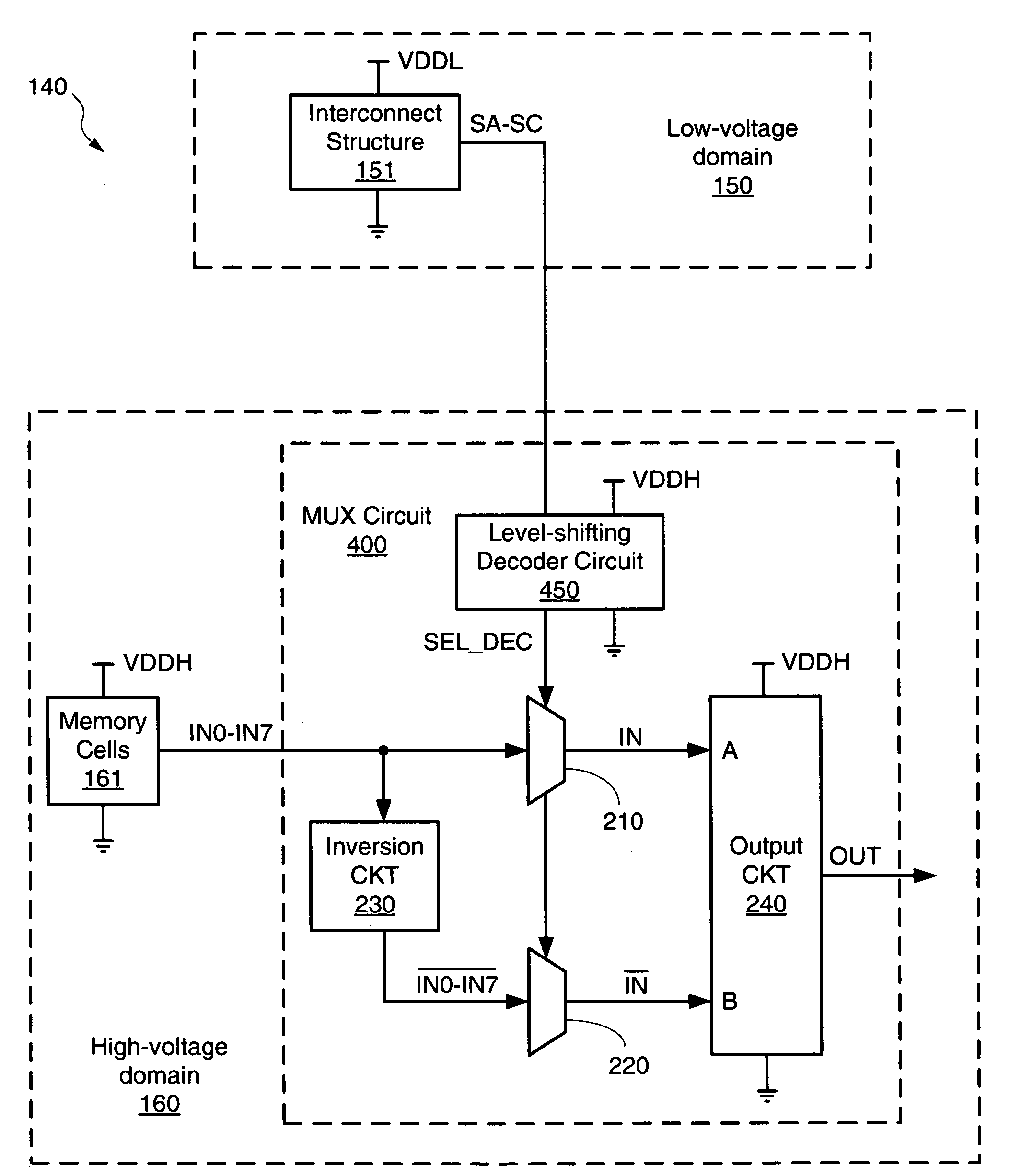
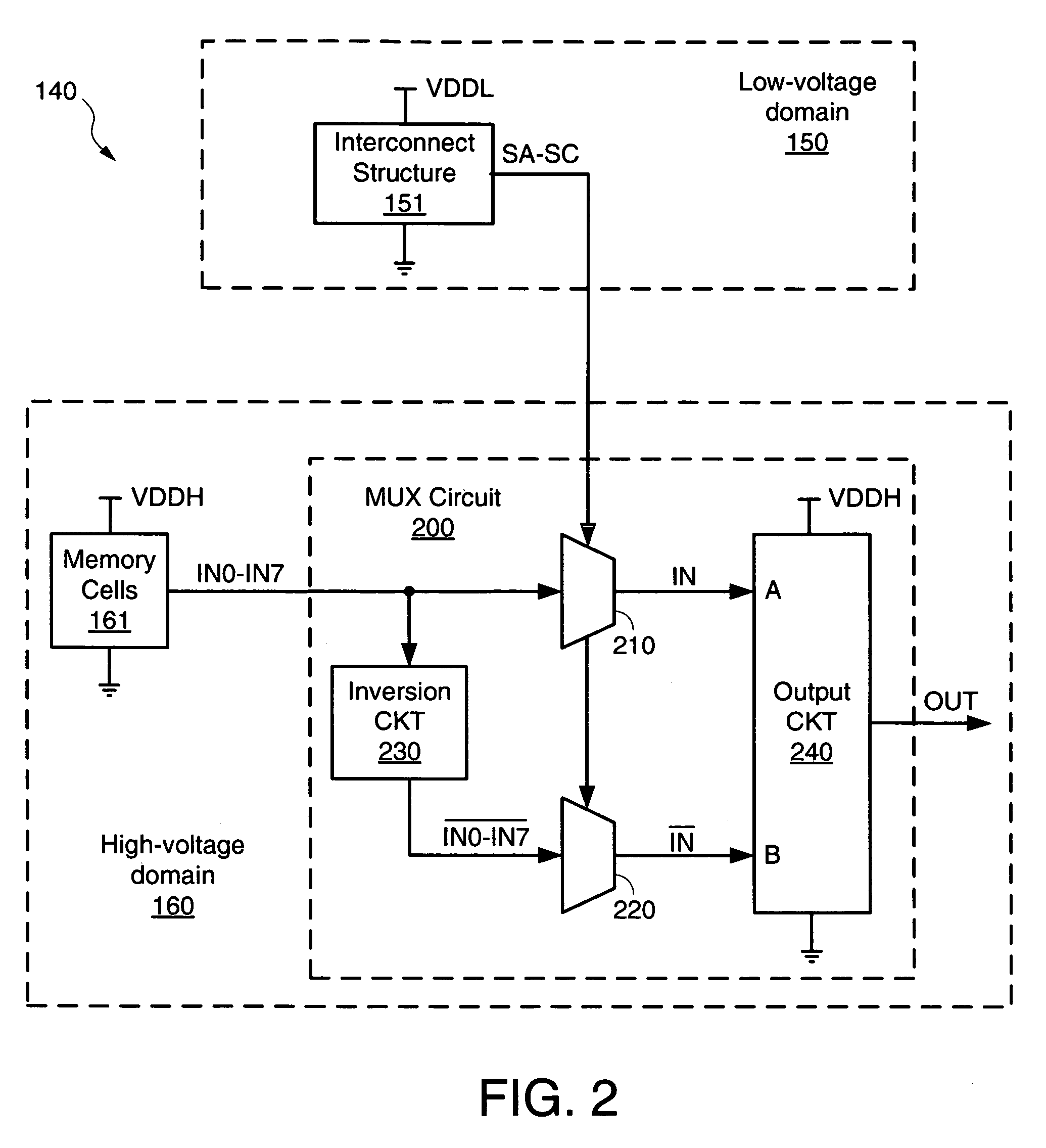
[0029]FIG. 2 shows an IC device 140 including a pseudo-differential multiplexer circuit 200 in accordance with first embodiments of the present invention. IC device 140, which may be any suitable IC device, includes a low-voltage domain 150 and a high-voltage domain 160. Low-voltage domain 150 is powered by a relatively low supply voltage VDDL...


PUM


Abstract

The present invention incorporates level-shifting functions within a multiplexer circuit that may be implemented in IC devices having low and high voltage domains. The multiplexer circuit utilizes pseudo-differential multiplexing architectures and employs level-shifting techniques to convert low-voltage signals received from the low-voltage domain into high-voltage signals more suitable for controlling the propagation of a selected input signal through the pass gates of the multiplexer circuit. For some embodiments, some of the select signals may be decoded to generate a number of decoded select signals that can be used to control the selective routing of signals through the multiplexer.

Description

FIELD OF INVENTION[0001]This invention relates generally to multiplexer circuits, and more particularly to multiplexer circuits capable of level-shifting logic signals.DESCRIPTION OF RELATED ART[0002]Multiplexer circuits are very common in integrated circuits (ICs) and other electronic circuits. For example, multiplexer circuits are used throughout many programmable logic devices (PLDs), such as field programmable gate arrays (FPGAs) and complex programmable logic devices (CPLDs), to programmably select one of several different input signals to pass to a logic destination, or to select one of several stored values to provide as the output signal from a lookup table (LUT). Therefore, multiplexers can form a significant portion of the logic circuitry in a PLD.[0003]FIG. 1 illustrates a well-known 8-to-1 binary multiplexer (MUX) circuit 100. A similar MUX architecture is commonly used to implement look-up tables (LUT) that form function generators in the configurable logic blocks of an...

Claims


Application Information

Patent Timeline
Patent Type & Authority Patents(United States)
IPC IPC(8): H03K19/173G06F7/38
CPCH03K17/005H03K17/693H03K19/01818
Inventor RAHMAN, ARIFURKAO, SEAN W.
Owner XILINX INC
Why Eureka
Try Eureka