

Method and circuit for collecting memory failure information
a technology of memory failure and information collection, applied in the field of integrated circuit testing, can solve the problems of inability to transfer raw detailed failure information without transformation, difficult or even impossible to do so in real time, and inability to achieve desirable or even possible transformation, so as to achieve the effect of reducing the amount of information to transfer
- Summary
- Abstract
- Description
- Claims
- Application Information
AI Technical Summary
Benefits of technology
Problems solved by technology
Method used
Image

Examples
example
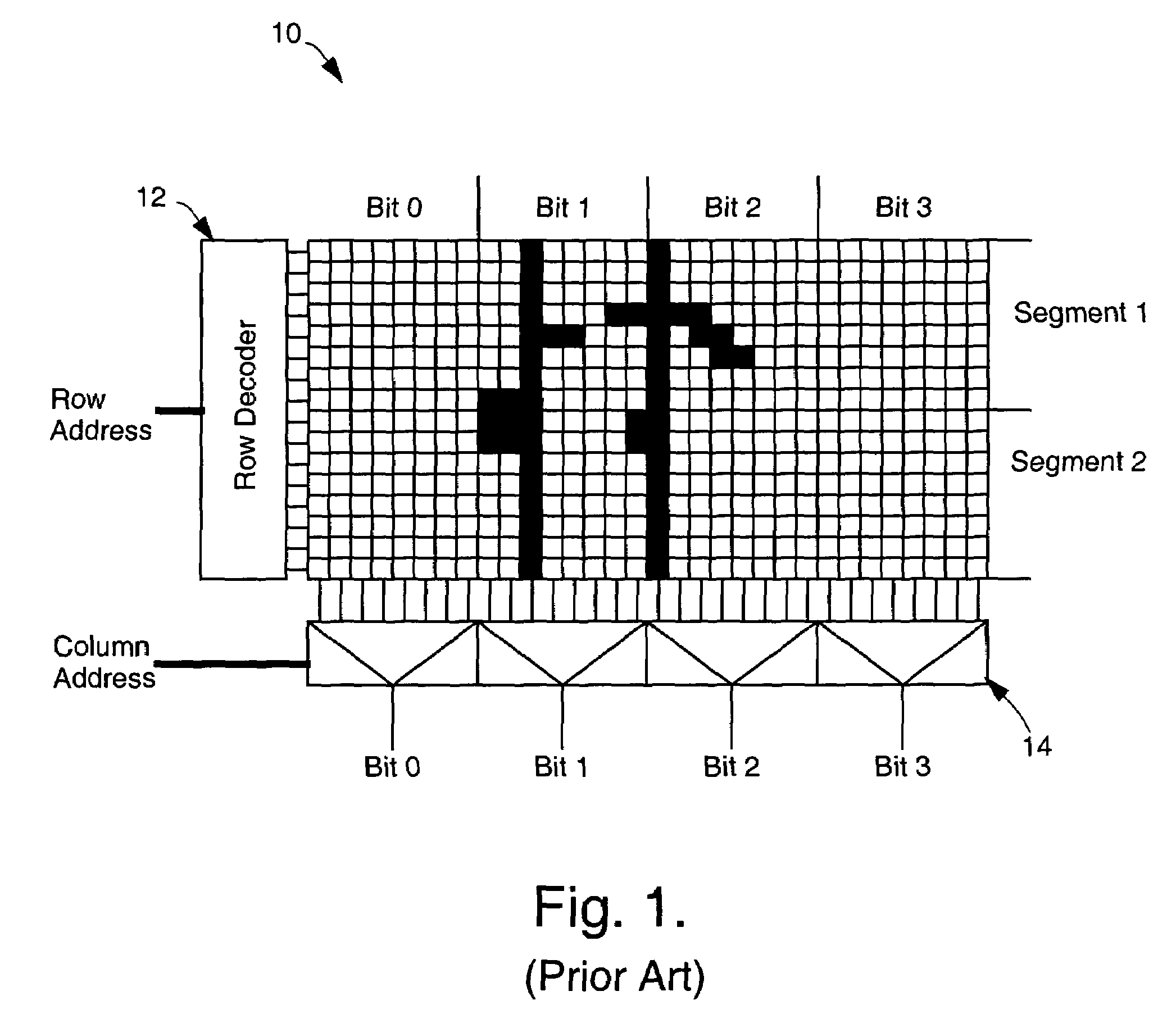
[0104]FIG. 14 illustrates an example of bitmaps and failure summaries generated for the memory shown in FIG. 1. For purposes of illustration, it is assumed that all words of the memory have 16 bits (bits 0 to 15). Only the first 16 rows of the memory are shown. The actual number of rows is typically 256 or more. It is assumed that there are no failures in rows below row 16. The number of rows and columns is not important.
[0105]The figure illustrates the results of a test which included making three passes of a test algorithm that has two phases in which the first phase uses a column access mode and the second phase uses a row access mode. It will be noted that a second or more passes are performed only if there are ambiguities due to more than one bit having failures and that one or more of the bits have a large number of failures at the same column address. The failure summary combination of FIG. 4 was used to collect failure summary data. FIG. 14(e) shows the actual column failure...
PUM
 Abstract
Description
Claims
Application Information