Method of manufacturing microlens, microlens, microlens array, electro-optical device, and electronic apparatus

a manufacturing method and technology of microlens, applied in the field of manufacturing microlens, microlens, microlens array, electrooptical devices, electronic devices, can solve the problems deteriorating significantly, and enhancing light usage efficiency, so as to reduce reduce the size, and reduce the effect of reducing the life of liquid crystal devices

Inactive Publication Date: 2008-05-13
SEIKO EPSON CORP
View PDF2 Cites 50 Cited by
  • Summary
  • Abstract
  • Description
  • Claims
  • Application Information

AI Technical Summary

Benefits of technology

[0009]An advantage of the invention is that it provides a method of manufacturing a microlens capable of suppressing a reduction of the lifetime of a liquid crystal device or the like due to light focused on one point without sacrificing display performance, such as luminance and contrast, and it provides the microlens, a microlens array, an electro-optical device, and an electronic apparatus.
[0010]According to an aspect of the invention, a method of manufacturing a microlens includes: forming on a transparent substrate an etching stop layer in a lens formation region where a curved lens surface of the microlens is to be formed, the etching stop layer having an island shape as a planar shape thereof; forming an intermediate layer on the etching stop layer; forming an etching mask layer on the intermediate layer, the etching mask layer having an opening at a position facing the etching stop layer; and etching, by means of isotropic etching, the intermediate layer from the opening, and etching the transparent substrate and the intermediate layer from a side of the etching stop layer.
[0011]According to the method of manufacturing the microlens of the invention, an etching stop layer is first formed within a lens formation region on a transparent substrate, such as a quartz substrate or a glass substrate. The etching stop layer has an island shape as a planar shape, on the transparent substrate, and for example, has a smaller size than a lens formation region when the microlens is finally formed through an etching process to be described later. Also, when curved lens surfaces of a plurality of microlens are formed on the transparent substrate, a plurality of etching stop layers dotted in island shapes is formed to correspond to positions of the plurality of microlens which is finally formed.
[0012]Subsequently, an intermediate layer is formed on the etching stop layer. The intermediate layer is formed using a general-purpose film formation method such as a CVD method or a sputtering method. Subsequently, an etching mask layer formed with an opening is formed at a position facing the etching stop layer on the intermediate layer. For example, the etching mask layer may be directly formed on the intermediate layer so as to avoid the position facing the etching stop layer. Also, the opening is formed, for example, by forming the etching mask layer so as to cover the entire intermediate layer and then removing a region including the position facing the etching stop layer. As such, after forming the etching stop layer, the intermediate layer, and the etching mask layer on the transparent substrate, the intermediate layer is etched from the opening by an isotropic etching, and the transparent substrate is also etched together with the intermediate layer from a side of the etching stop layer. Specifically, the etching stop layer is exposed as the intermediate layer is etched outward from the opening, and the transparent substrate, which is exposed from a side of the etching stop layer by removing the intermediate layer, is etched to thereby keep etching the intermediate layer.
[0013]As a result, a curved lens surface having the specific shape is formed in the transparent substrate by means of the presence of the etching stop layer. Specifically, an etched surface propagating toward an inside of the etching stop layer from the side of the etching stop layer becomes in contact with a lower position of the etching stop layer to form a curved lens surface which is convex toward the etching stop layer. On the other hand, an etched surface propagating toward an outside of the etching stop layer forms a curved lens surface which is convex at a position opposite to the curved lens surface formed at the lower position of the etching stop layer. Since the transparent substrate is etched from the side of the etching stop layer and the lower position of the etched intermediate layer, the above-described curved lens surface constitutes one curved lens surface which is continuously connected in the lens formation region of the transparent substrate.
[0014]When the resultant curved lens surface is filled with a resin having an optical transmitting property, a microlens can be formed in which a central portion is more pitted than the circumferential portion. Such a microlens can make both of the central portion of the lens, which is more pitted than circumference, and the circumferential portion around the central portion act as lenses. In addition, light emitted from the light source can be focused on the pixel region by means of the specific curved lens surface, while light can be properly dispersed so as not to make them focused on one point of the pixel region. Accordingly, deterioration of each part of the pixel region due to light focused on one point can be suppressed without sacrificing the optical transmittance in the pixel region. By means of this, the orientation layer within the pixel region can be suppressed from being deteriorated, and a lifetime of the liquid crystal device can increase. Moreover, the etched surface of the etched transparent substrate can be used as the curved lens surface for the microlens without filling the etched surface with a resin or the like.

Problems solved by technology

However, when a microlens is employed, typically, light emitted from the light source is locally focused via the microlens on a portion positioned at the center of an opening region of each pixel, for example, of a liquid crystal or an orientation layer: the inventors have found that deterioration was significant in this portion.
Furthermore, the inventors expect that the lens characteristics of the microlens are not good because the central portion of the microlens is flat.
Accordingly, it is difficult to enhance the light usage efficiency by effectively focusing light within the opening region, so that it is difficult to enhance the display luminance and contrast.

Method used


Image

  • Method of manufacturing microlens, microlens, microlens array, electro-optical device, and electronic apparatus
  • Method of manufacturing microlens, microlens, microlens array, electro-optical device, and electronic apparatus
  • Method of manufacturing microlens, microlens, microlens array, electro-optical device, and electronic apparatus

Examples


Embodiment Construction

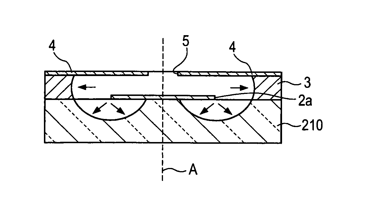
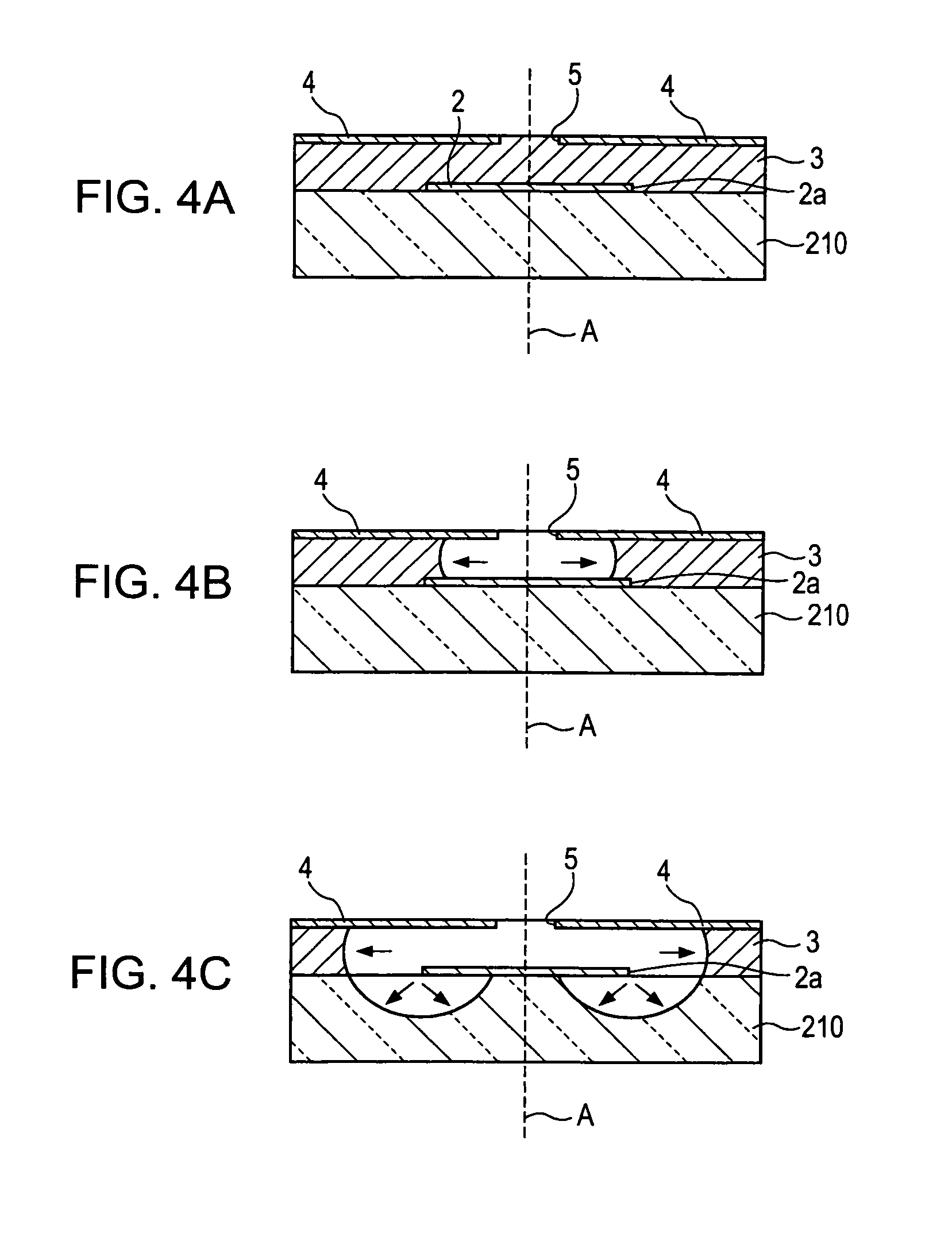
[0069]Hereinafter, a microlens manufacturing method, a microlens, a microlens array, an electro-optical device, and an electronic apparatus in accordance with the invention will be described in detail with reference to the accompanying drawings.

Microlens Array Plate

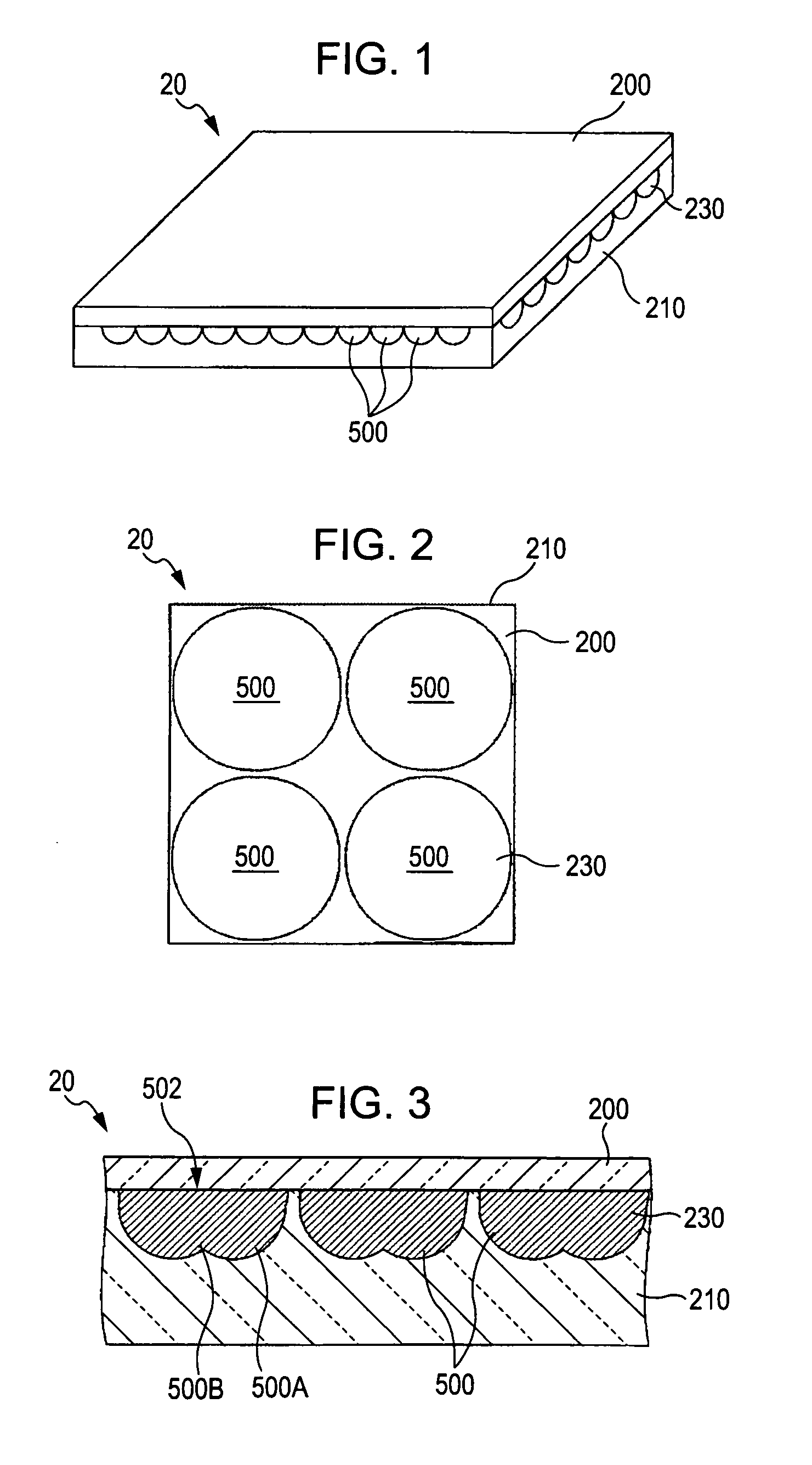
[0070]First, a microlens plate to which a microlens according to the invention is applied will be described with reference to FIGS. 1 to 3. FIG. 1 is a perspective view schematically illustrating a microlens array plate according to the present embodiment. FIG. 2 is an enlarged plan view illustrating a part associated with four adjacent microlenses among microlenses included in the microlens array plate. FIG. 3 is an enlarged view illustrating a part of the cross-section of the microlens array plate in accordance with the present embodiment.

[0071]Referring to FIG. 1, the microlens array plate 20 of the present embodiment is configured to include a plurality of microlenses 500 which are arranged in a planar matrix on a tra...


PUM

PropertyMeasurementUnit
refractive indexaaaaaaaaaa
transparentaaaaaaaaaa
sizeaaaaaaaaaa

Abstract

A method of manufacturing a microlens includes: forming on a transparent substrate an etching stop layer in a lens formation region where a curved lens surface of the microlens is to be formed, the etching stop layer having an island shape as a planar shape thereof; forming an intermediate layer on the etching stop layer; forming an etching mask layer on the intermediate layer, the etching mask layer having an opening at a position facing the etching stop layer; and etching, by means of isotropic etching, the intermediate layer from the opening, and etching the transparent substrate and the intermediate layer from a side of the etching stop layer.

Description

BACKGROUND OF THE INVENTION[0001]1. Technical Field[0002]The present invention relates to a microlens used for an electro-optical device such as a liquid crystal device, to a microlens array, to a method of manufacturing the same, and to an electro-optical device, and to an electronic apparatus having microlenses.[0003]2. Related Art[0004]In an electro-optical device such as a liquid crystal device, for example, a microlens corresponding to each pixel is formed on a counter substrate or a microlens array plate including a plurality of microlenses is bonded to the counter substrate. By using such a microlens array, a bright display can be realized in an electro-optical device. That is, the microlenses increase the usage efficiency of light emitted from a light source by causing the light emitted from the light source, such as a backlight, to be focused on an opening region of each pixel without wasting any light. For example, a liquid crystal device including such microlenses is manu...

Claims


Application Information

Patent Timeline
Patent Type & Authority Patents(United States)
IPC IPC(8): G02B27/10B29D11/00
CPCG02B3/0012G02B3/0056G02F1/133526Y10S359/90G02B3/00G02F1/1335
Inventor OZAWA, NORIHIKO
Owner SEIKO EPSON CORP
Why Eureka
Try Eureka