Rate adaption within a TDM switch using bit stuffing

a tdm switch and rate adaptation technology, applied in the field of data nodes in communication networks, can solve the problems of unstable fll, inability to transmit data with the data clock, and very limited number of output frequencies, so as to prevent the introduction of bit loss, improve the jitter and frequency stability, and improve the effect of fll stability

Inactive Publication Date: 2008-05-13
TELEFON AB LM ERICSSON (PUBL)
View PDF16 Cites 3 Cited by
  • Summary
  • Abstract
  • Description
  • Claims
  • Application Information

AI Technical Summary

Benefits of technology

[0034]In particular, the present invention discloses a method and an arrangement providing transmission of data through a node, e.g. a switch. At the receiving side of the switch, one extra bit per frame is transferred over the time slot bus of the switch if the number of bits in the corresponding FIFO of the input line exceeds a predefined upper limit. In contrast, one bit less per frame is transferred if the number of bits in the corresponding FIFO of the input line goes below a predefined lower limit. At the transmitting side of the switch, a FLL circuit regulates the data rate out of the FIFOs. The FLL circuit is implemented as a P-regulator having i.a. the fill degree of the is FIFO as a direct input. The present invention prevents introduction of bit loss, still maintaining the nominal bit rate in spite of a very simple and flexible implementation. The FLL circuit provides excellent jitter and frequency stability, and because of not using an I-component, the FLL circuit becomes stable.

Problems solved by technology

It is not possible to transmit data with the data clocks.
Since the receiving lines are independent in relation to data speed and timing, it is also a challenge to transmit data on the same data bus without introducing data and timing faults.
The disadvantages with such a PI-regulator are:
The I-component can make the FLL unstable.
The number of output frequencies is then very limited.
Such frequency jumps introduce wander in the system.
This is a problem since wander is more difficult to attenuate than jitter.
Besides, the side channel for transferring timing information has a fixed bandwidth, and the multiframe structure is quite complicated.
Because of the multiframe structure, timing information can not be updated for each frame.
The way the RX FIFO-Digital FLL solution uses threshold values to control the rate of the output clock does not give optimal jitter and stability characteristics on the output frequency.
Generally, problems with the known way of signalling timing faults described in the chapter above is that since the CPU must be involved, the action may be relatively long lasting and some of the CPU capacities become occupied.

Method used


Image

  • Rate adaption within a TDM switch using bit stuffing
  • Rate adaption within a TDM switch using bit stuffing
  • Rate adaption within a TDM switch using bit stuffing

Examples


Embodiment Construction

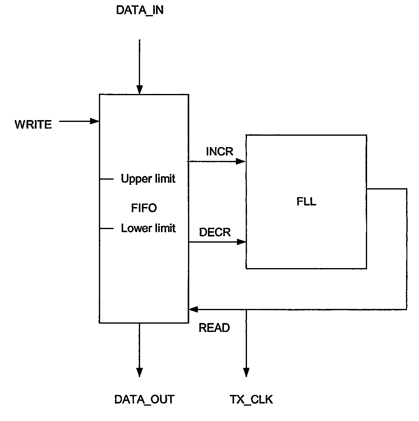
[0042]In order to achieve bit transparent pipes with independent timing, the present invention proposes a method inserting a certain header in each frame before transmission on the TDM bus. Also according to the present invention, a FIFO for each output port at the transmitting side of the switch is regulated with inventive regulation circuits.

[0043]At the receiving side of the switch there is a FIFO for each input port with a programmable depth, e.g. 64 bits, and the serial data of the input lines is clocked into the FIFOs. An example of such FIFO can be, seen in FIG. 4. As it can be seen from FIG. 4, the FIFO depth may be less than the actual physical size. It should be possible to reset the FIFO pointer to a mid-position. This is preferably done automatically when there is an overflow or underflow error in the FIFO, or the software programmer can do it at any time.

[0044]The abovementioned header is, i.a., used for bit stuffing. Bit stuffing in this context is used to compensate f...


PUM


Abstract

The present invention discloses a method and an arrangement providing transmission of data through a node, e.g. a switch, having different input and output line interfaces in a wide range of data speed, without introducing any loss of bits, but still maintaining the nominal bit rate. This is achieved by means of a very simple and flexible implementation. At the receiving side of the switch, one extra bit per frame is transferred over the time slot bus of the switch if the number of bits in the corresponding FIFO of the input line exceeds a predefined upper limit. In contrast, one bit less per frame is transferred if the number of bits in the corresponding FIFO of the input line goes below a predefined lower limit. At the transmitting side of the switch, a FLL circuit regulates the data rate out of the FIFOs. The FLL circuit is implemented as a P-regulator having i.a. the fill degree of the FIFO as a direct input. Consequently, excellent jitter and frequency stability are achieved, and because of not using an I-component, the FLL circuit becomes stable.

Description

FIELD OF THE INVENTION[0001]The present invention is related to data nodes in communication networks, in particular to transmitting independent serial data streams through synchronous Time Division Multiplexing (TDM) switches.BACKGROUND OF THE INVENTION[0002]The lower layer of communication networks like the connectivity layer in a core network of a cellular environment could be seen as a layer of distributed resources for managing data flows. Switches and multiplexers are some of the main components for this purpose. In complex communication networks managing data of different formats and varying data rates, it is of great importance that the construction of the components is flexible without being too complex.[0003]Conventionally, the switches comprise a number of serial inputs and outputs. The data stream of one input may be directed in its entirety to a certain output line, or it may consist of a mixture of time division multiplexed data frames that are to be distributed to seve...

Claims


Application Information

Patent Timeline
Patent Type & Authority Patents(United States)
IPC IPC(8): H04L12/28G06F13/00H02JH04L7/02H04L12/56H04Q11/04
CPCH04J3/0623
Inventor WEGO, ARILDHELLUM, PAL LONGVA
Owner TELEFON AB LM ERICSSON (PUBL)
Why Eureka
Try Eureka