Laser irradiation apparatus and method for manufacturing semiconductor device

a laser irradiation and semiconductor technology, applied in the direction of laser details, semiconductor devices, electrical devices, etc., can solve the problems of inconvenient resetting of optical systems, and inability to adjust optical systems in time, so as to shorten the time for readjusting optical systems, shorten the time, and improve the effect of heat resistan

Inactive Publication Date: 2008-05-20
SEMICON ENERGY LAB CO LTD
View PDF20 Cites 1 Cited by
  • Summary
  • Abstract
  • Description
  • Claims
  • Application Information

AI Technical Summary

Benefits of technology

[0023]In view of the above problem, it is an object of the present invention to provide a laser irradiation apparatus that can readjust the optical system more easily and more accurately than the conventional technique in which the steering mirror is used and that can shorten the time for readjusting the optical system to a large degree. Moreover, it is also an object of the present invention to provide a method for manufacturing a semiconductor device using the laser irradiation apparatus.
[0047]Conventionally, when the laser beam is displaced from the predetermined position, the misalignment is corrected by readjusting the optical system including a plurality of steering mirrors. Such a conventional method requires much time until the apparatus can be used again. According to the present invention, however, only one optical element is readjusted to correct the misalignment of the laser beam from the predetermined position. Therefore, it is possible to shorten the time for readjusting the optical system. Moreover, unlike the steering mirror, the present invention does not affect the traveling direction, and therefore the misalignment of the laser beam can be corrected easily without considering the change of the traveling direction.
[0048]As thus described, since the misalignment of the laser beam from the predetermined position can be corrected easily in short time by the present invention, the laser irradiation apparatus can be used again in short time after the maintenance work inside the laser oscillator. Therefore, the present invention can avoid waste of time and can increase the throughput.

Problems solved by technology

This is because an inexpensive glass substrate, which is often employed as a substrate of a TFT, is inferior in heat resistance and is easy to change in shape due to heat.
However, in this method, adjustment of the optical system requires a large amount of time.
For this reason, very accurate readjustment of the optical system is required, which consumes a large amount of time.
This causes the throughput to decrease.
Particularly, the optical system is most frequently readjusted when the laser beam is displaced from the predetermined position due to the maintenance work inside the laser oscillator.
In this case, it is difficult to set the window to the same place and the window may be displaced.
Therefore, when the laser beam is displaced from the predetermined position, the laser beam is incident into a different position in the optical system, and the intensity distribution of the beam spot formed on the irradiated surface may not be homogeneous.
As a result, the annealing may not be performed homogeneously to the irradiated object.
However, the method using the steering mirror has the following problem.
Thus, the conventional technique in which two steering mirrors are used to correct the misalignment of the laser beam from the predetermined position has a problem to be solved.
Although the misalignment of the laser beam from the predetermined position can be corrected by readjusting the optical system, this method is not preferable because the readjustment requires high accuracy and consumes a large amount of time as described above.

Method used


Image

  • Laser irradiation apparatus and method for manufacturing semiconductor device
  • Laser irradiation apparatus and method for manufacturing semiconductor device
  • Laser irradiation apparatus and method for manufacturing semiconductor device

Examples


embodiment mode 1

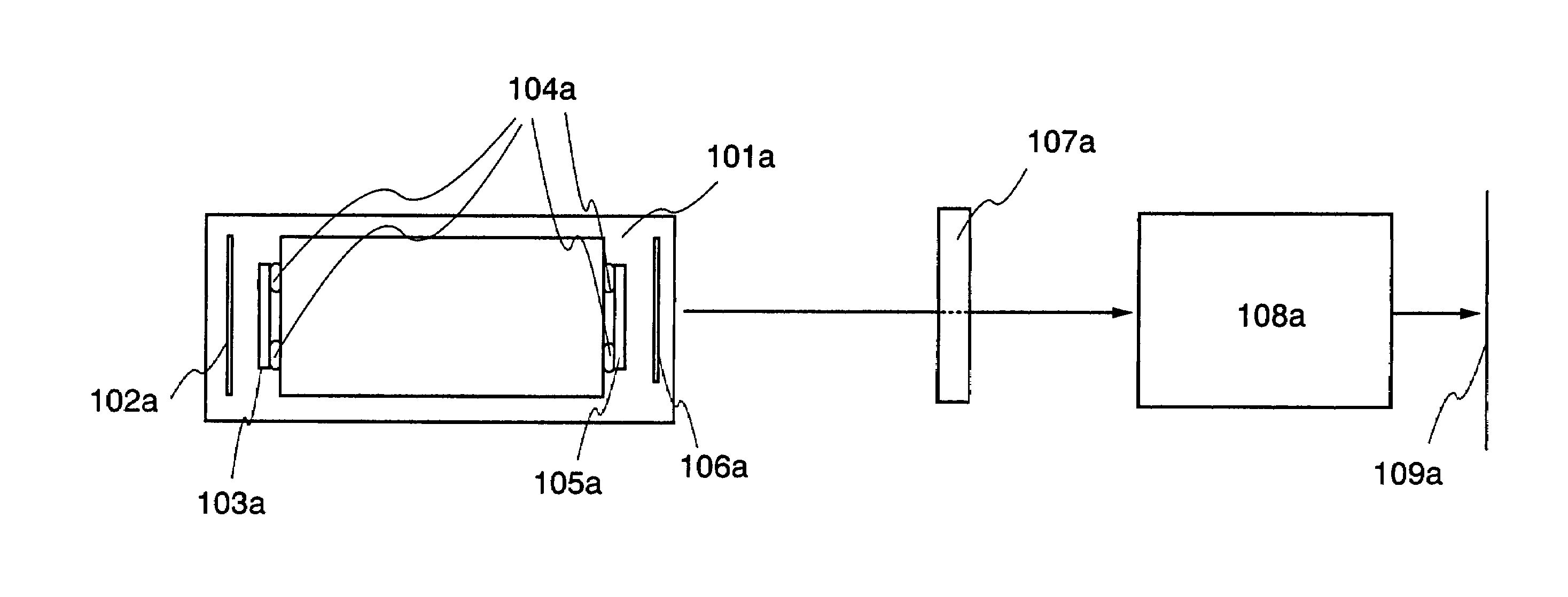
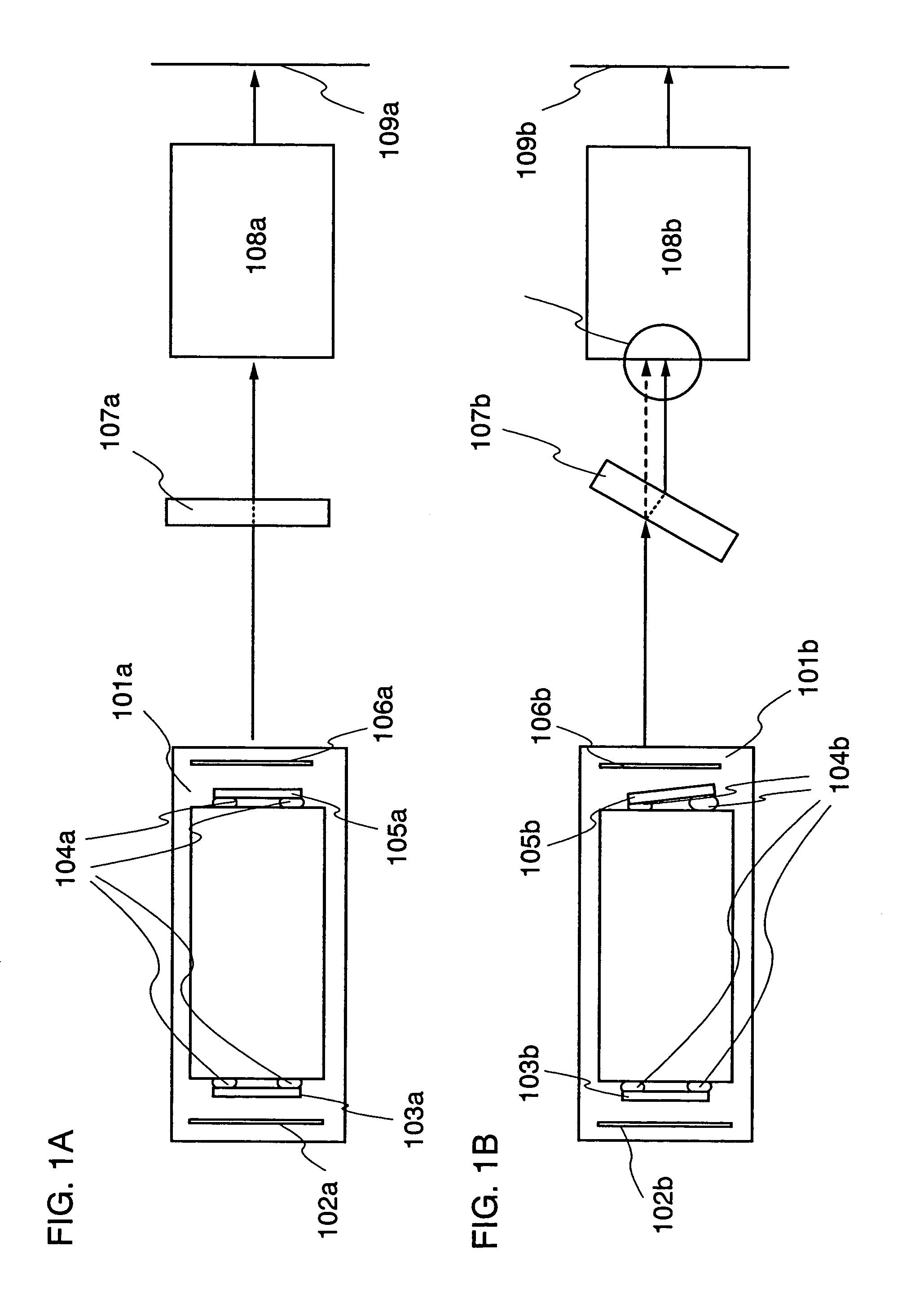
[0062]An embodiment mode of the present invention is explained with reference to FIGS. 1A and 1B. FIGS. 1A and 1B show an example in which the misalignment of the laser beam from the predetermined position is corrected using a flat glass. Both figures show schematically an internal structure of an excimer laser, which is one kind of gas laser. The gas laser typified by the excimer laser has a window, a mirror, and the like inside, and it is necessary to perform the maintenance work such as cleaning of these parts regularly. This embodiment mode explains an example in which a flat glass is used to correct a misalignment of the laser beam from a predetermined position that is caused by the maintenance work in which the parts are removed for the cleaning and then the parts are set again.

[0063]In FIGS. 1A and 1B, the laser irradiation apparatus has the same laser oscillator and the same optical system by which a beam spot having a homogeneous intensity distribution is formed on an irrad...

embodiment mode 2

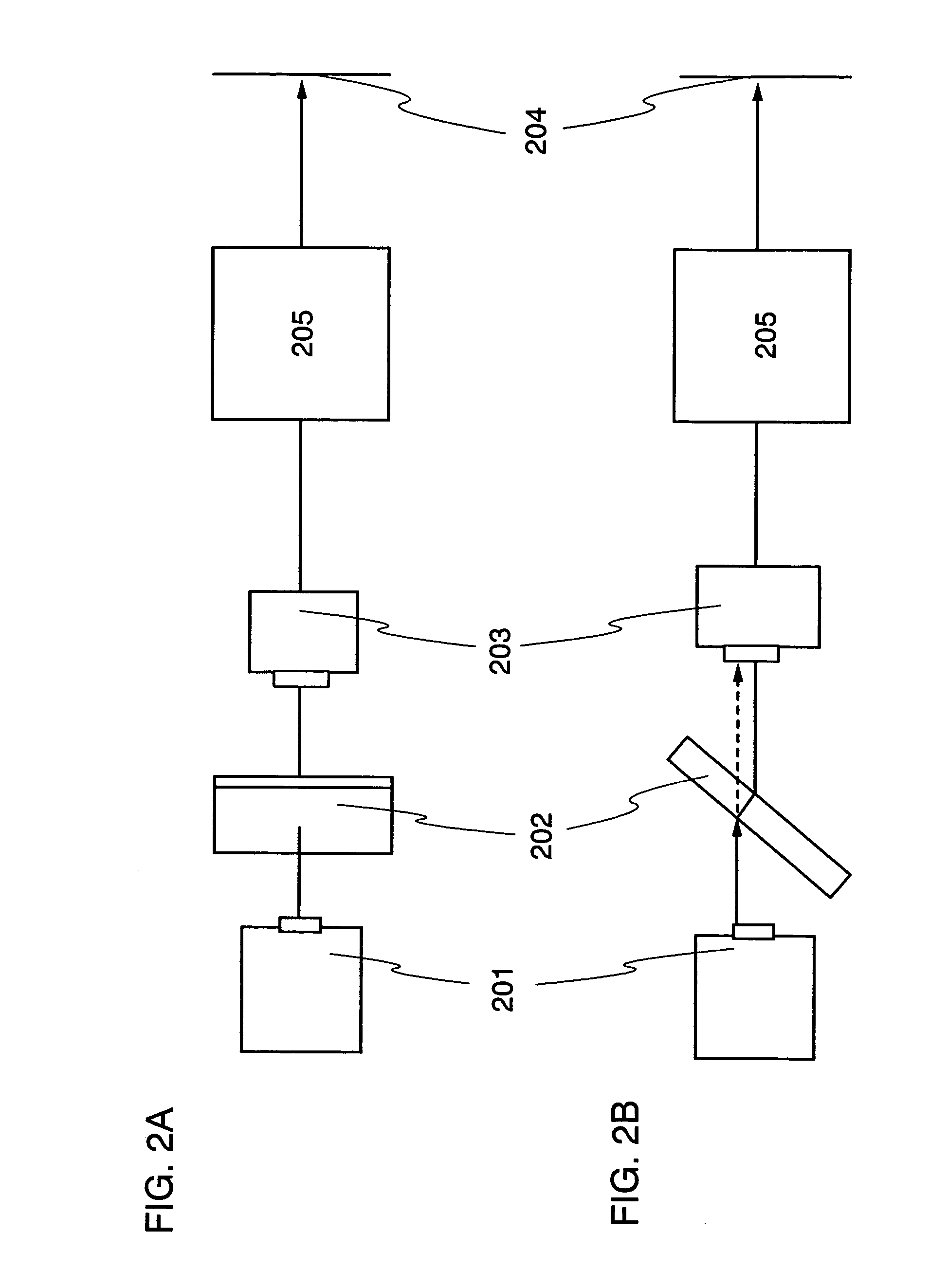
[0067]The present embodiment mode explains with reference to FIGS. 2A and 2B an example in which a CCD camera is used in addition to the flat glass explained in the embodiment mode 1. The CCD camera records a predetermined position of a laser beam before the laser beam is displaced from the predetermined position. After the laser beam is displaced, the misalignment is detected by using the CCD camera again.

[0068]In FIGS. 2A and 2B, the laser irradiation apparatus has an optical system 205 for forming a rectangular beam spot having a homogeneous intensity distribution on an irradiated surface 204. A beam spot having a rectangular shape on the irradiated surface is hereinafter referred to as a rectangular beam. This optical system 205 may be designed appropriately by a practitioner in accordance with the size, shape, and the like of the beam spot that the practitioner desires to form on the irradiated surface.

[0069]An excimer laser is used as a laser oscillator 201 as well as in the e...

embodiment 1

[0073]This embodiment explains an example of the laser irradiation and shows the specific optical system with reference to FIGS. 3A and 3B. In FIGS. 3A and 3B, an excimer laser is used as a laser oscillator 301. The optical system has cylindrical lens arrays 303 and 304, convex cylindrical lenses 305 and 306, and a doublet cylindrical lens 307 consisting of cylindrical lenses 307a and 307b. This optical system is used to form a laser beam having a rectangular shape on an irradiated surface 308. Hereinafter this laser beam is referred to as a rectangular beam. It is noted that a direction of a long side of the rectangular beam formed on the irradiated surface 308 is perpendicular to the paper in FIG. 3A.

[0074]In FIG. 3A, the laser beam incident into the cylindrical lens array 303 is divided in a direction of a short side of the rectangular beam, and the divided beams are combined by the convex cylindrical lens 305. Thus, the intensity distribution is homogenized in the direction of t...


PUM


Abstract

The linear laser beam generally has a width of 1 mm or less, and it is necessary to adjust the optical system with high accuracy in order to form the laser beam having such a narrow width and having a homogeneous intensity distribution. The adjustment of the optical system requires a large amount of time, and the laser irradiation apparatus using this optical system cannot be used during the adjustment of the optical system. This causes the throughput to decrease. The present invention is made to facilitate a readjustment of the optical system and to shorten the time required for it. When the misalignment of the laser beam is corrected to keep the incident position in the optical system the same by moving the laser beam parallel with the use of a single optical element, it is no longer necessary to readjust all the optical elements, and therefore the time can be saved.

Description

BACKGROUND OF THE INVENTION[0001]1. Field of the Invention[0002]The present invention relates to a laser irradiation apparatus and a method for manufacturing a semiconductor device by using the laser irradiation apparatus.[0003]2. Related Art[0004]In recent years, a technique to form a thin film transistor (hereinafter referred to as a TFT) over a substrate has made great progress, and application development to an active matrix display device has been advanced. Particularly, a TFT formed using a poly-crystalline semiconductor film is superior in field-effect mobility to a TFT formed using a conventional amorphous semiconductor film, and therefore high-speed operation becomes possible when the TFT is formed using the poly-crystalline semiconductor film. For this reason, a circuit for driving a pixel, which has been mounted by an external IC chip, can be formed integrally with the pixel over the same substrate by a TFT.[0005]The poly-crystalline semiconductor film suitable for manufa...

Claims


Application Information

Patent Timeline
Patent Type & Authority Patents(United States)
IPC IPC(8): H01L21/20H01L21/268H01L21/77H01L21/84H01S3/10
CPCH01L21/268H01L27/1214H01L27/1285H01L27/1277
Inventor TANAKA, KOICHIRO
Owner SEMICON ENERGY LAB CO LTD
Why Eureka
Try Eureka