Vertical memory device structures

a memory device and vertical technology, applied in the direction of semiconductor devices, semiconductor/solid-state device details, radiation controlled devices, etc., can solve the problems of increasing the cost of manufacturing equipment and technology required to support the manufacture of such highly integrated chips with each new generation of smaller devices

Active Publication Date: 2008-05-27
BESANG
View PDF1 Cites 352 Cited by
  • Summary
  • Abstract
  • Description
  • Claims
  • Application Information

AI Technical Summary

Problems solved by technology

These laterally oriented devices consume significant amounts of chip area.
However, the manufacturing equipment and technologies required to support the manufacture of such highly integrated chips becomes increasingly expensive with each new generation of smaller devices.

Method used


Image

  • Vertical memory device structures
  • Vertical memory device structures
  • Vertical memory device structures

Examples


Embodiment Construction

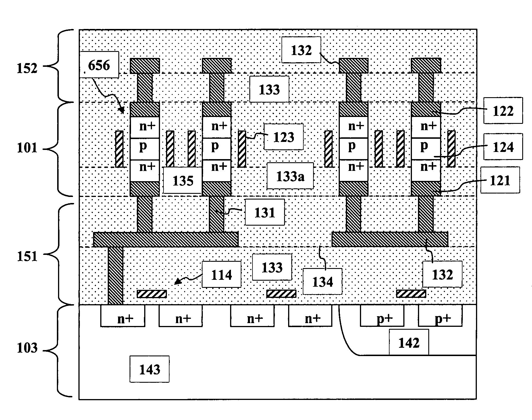
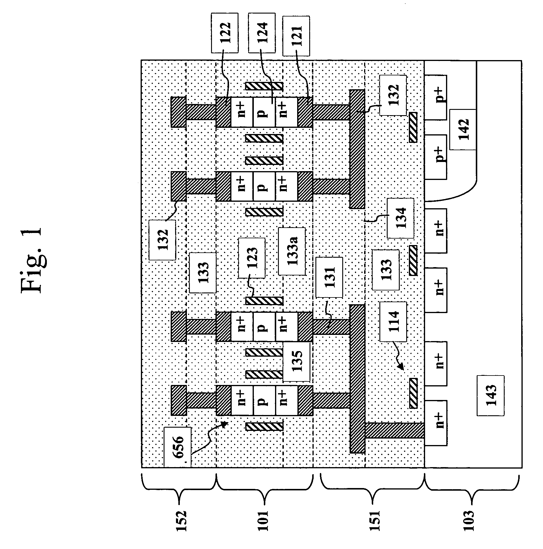
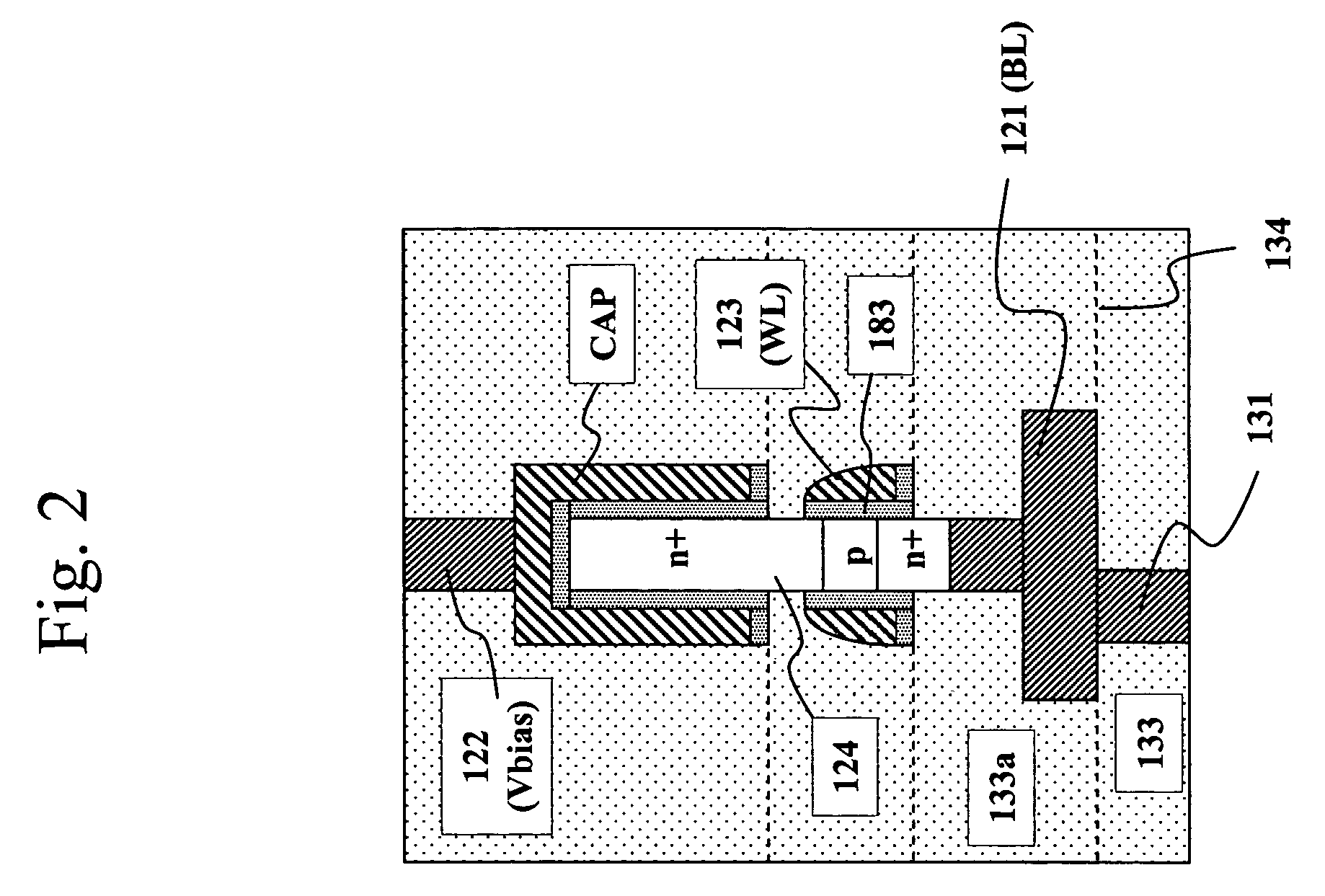
[0042]Vertically oriented memory structures constituting memory cells, or portions thereof, in a 3-D integrated circuit arrangement in accordance with the present invention, are shown in FIG. 1. Embodiments of the present invention provide a device integration architecture and technology. More particularly, memory cells, or portions thereof, which are vertically oriented with respect to a major surface of a wafer, are provided so that the effective device density, i.e., devices per unit area of the wafer surface, is increased. In this way, greater functionality can be provided in a chip of a given surface area.

[0043]Reference herein to “one embodiment”, “an embodiment”, or similar formulations, means that a particular feature, structure, operation, or characteristic described in connection with the embodiment, is included in at least one embodiment of the present invention. Thus, the appearances of such phrases or formulations herein are not necessarily all referring to the same emb...


PUM


Abstract

Vertically oriented semiconductor memory cells are added to a separately fabricated substrate that includes electrical devices and / or interconnect. The plurality of vertically oriented semiconductor memory cells are physically separated from each other, and are not disposed within the same semiconductor body. The plurality of vertically oriented semiconductor memory cells can be added to the separately fabricated substrate as a thin layer including several doped semiconductor regions which, subsequent to attachment, are etched to produce individual doped stack structures, which are then supplied with various dielectric coatings, gate electrodes, and contacts by means of further processing operations. Alternatively, the plurality of vertically oriented semiconductor memory cells may be completely fabricated prior to attachment. DRAMs, SRAMs, non-volatile memories, and combinations of memory types can be provided.

Description

CROSS REFERENCE TO RELATED APPLICATIONS[0001]This is a continuation-in-part of application Ser. No. 10 / 873,969, entitled “Three-Dimensional Integrated Circuit Structure and Method of Making Same”, filed 21 Jun. 2004; and which is incorporated in its entirety herein by reference.FIELD OF THE INVENTION[0002]The present invention relates generally to semiconductor structures and manufacturing methods for memory devices and circuits. More particularly, the present invention relates to a semiconductor substrate combined with a relatively thin add-on semiconductor layer in which various vertically oriented memory elements are fabricated.BACKGROUND OF THE INVENTION[0003]Advances in semiconductor manufacturing and digital systems architecture have provided the means to produce chips, or integrated circuits, with many millions of active and passive circuit elements along with the interconnects needed to create the desired circuit networks. As is well-known, integrated circuits contain transi...

Claims


Application Information

Patent Timeline
Patent Type & Authority Patents(United States)
IPC IPC(8): H01L27/108H01L21/20H01L21/30H01L21/336H01L21/46H01L21/58H01L23/48H01L27/148
CPCH01L21/2007H01L24/83H01L27/0688H01L27/11551H01L27/11556H01L24/29H01L2924/1305H01L2924/1301H01L2924/01033H01L2224/291H01L2224/8385H01L2924/01005H01L2924/01013H01L2924/01015H01L2924/01018H01L2924/01027H01L2924/01029H01L2924/01038H01L2924/01056H01L2924/01073H01L2924/01074H01L2924/01075H01L2924/01078H01L2924/01079H01L2924/07802H01L2924/13091H01L2924/14H01L2924/1433H01L2924/19041H01L2924/19042H01L2924/19043H01L2924/30105H01L2924/3011H01L2924/01006H01L2924/01019H01L2924/00H10B12/315H10B12/50H10B12/05H10B41/20H10B41/27
Inventor LEE, SANG-YUN
Owner BESANG
Why Eureka
Try Eureka