Unlock instant, AI-driven research and patent intelligence for your innovation.

Delay-locked loop circuit

a delay-locked loop and circuit technology, applied in the direction of electrical equipment, pulse automatic control, etc., can solve the problems of misoperation and increase in power consumption

Active Publication Date: 2008-05-27
TEXAS INSTR INC
View PDF1 Cites 5 Cited by
  • Summary
  • Abstract
  • Description
  • Claims
  • Application Information

AI Technical Summary

Benefits of technology

Prevents abnormal lock states at start-up and during operation, maintaining stable phase locking and reducing power consumption by ensuring the phase difference is within a desired range.

Problems solved by technology

In the DLL circuit shown in FIG. 22, control is performed such that phase difference Δφ between clock signal φin and clock signal φdin is “2π.” Consequently, when integer n changes, all of the signals output from the various delay elements of delay line 1 change, and this is a problem.
In the example shown in FIG. 28, the lock state shifts from point A shown in FIG. 27 to point C. For the DLL circuit, when operation continues in said abnormal lock state, the circuit that operates based on the clock signal generated by DLL circuit becomes unstable, so that mis-operation takes place, and the power consumption rises due to waste.
This is undesirable.

Method used


Image

  • Delay-locked loop circuit
  • Delay-locked loop circuit
  • Delay-locked loop circuit

Examples


embodiment 1

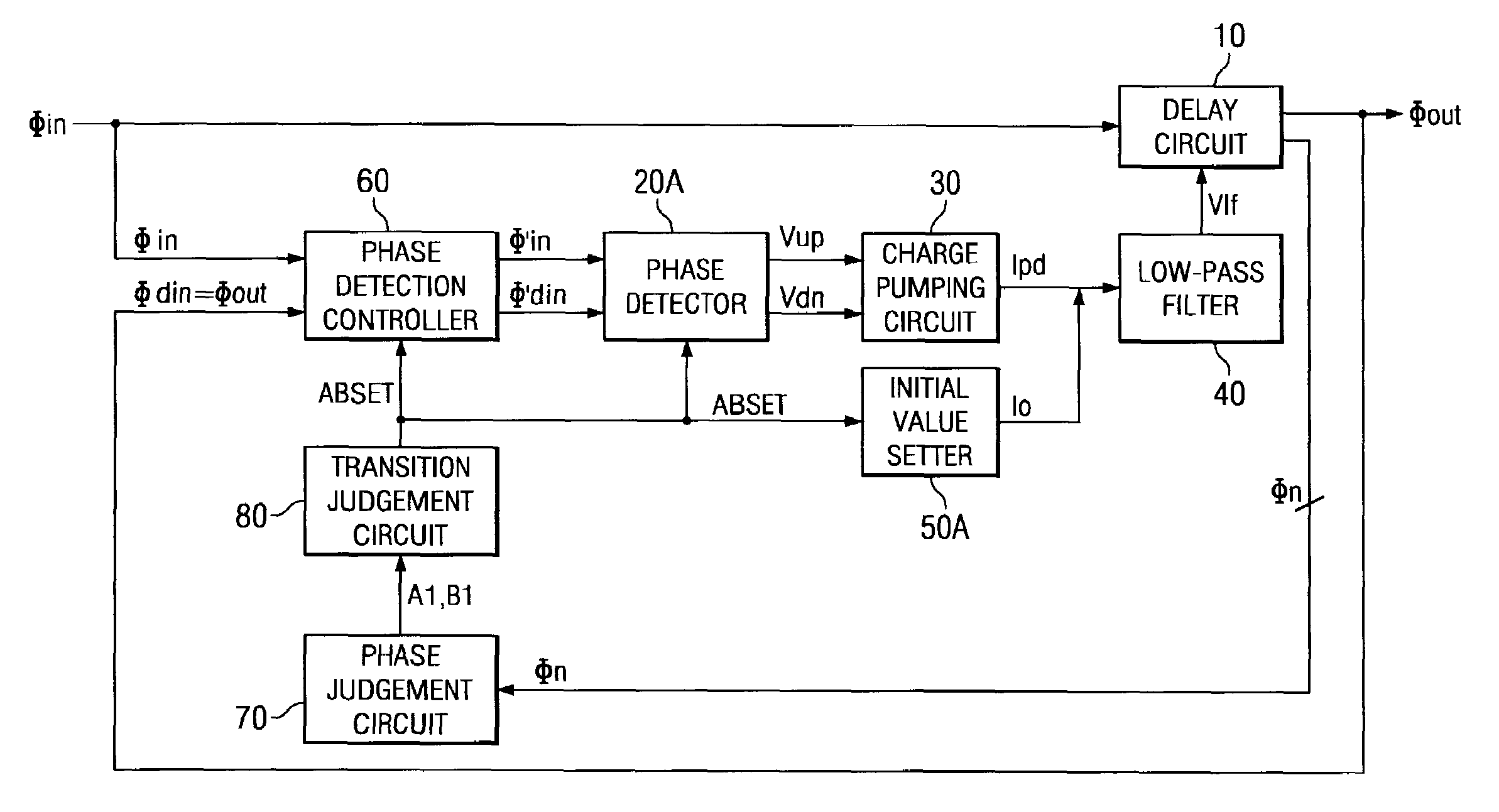
[0062]FIG. 1 is a diagram illustrating an example of the constitution of the DLL circuit pertaining to Embodiment 1 of the present invention. The DLL circuit shown in FIG. 1 has delay circuit 10, phase detector (phase comparator) 20, charge-pumping circuit 30, low-pass filter 40, initial value setter 50, and phase-detection controller 60. Said delay circuit 10 is an embodiment of the delay circuit of the present invention. Said phase detector (phase comparator) 20 is an embodiment of the phase detector (phase comparator) of the present invention. The circuit containing charge-pumping circuit 30, low-pass filter 40 and initial value setter 50 is an embodiment of the delay controller of the present invention. Said charge-pumping circuit 30 is an embodiment of the charge-pumping circuit of the present invention. Said low-pass filter 40 is an embodiment of the low-pass filter of the present invention. Said initial value setter 50 is one embodiment of initial value setter 50 of the prese...

embodiment 2

[0084]In the following, an explanation will be given regarding Embodiment 2 of the present invention. For the DLL circuit in Embodiment 2, it is checked whether the phase state of the delay signal generated in the delay circuit correctly changes, and, if an abnormal transition takes place, the DLL operation is paused and a prescribed initial state is set to correct the DLL operation. For example, when the lock locus is departed from due to the influence of external noise and variation in the frequency of clock signal φin, by correcting the DLL operation from an appropriate initial state, it is possible to prevent continuation of an abnormal locked state. For example, as shown in FIG. 27, when the initial phase difference in delay line 1 is “+2π”˜“+4π,” locking occurs at point A in the conventional DLL circuit. However, due to variation in the power source voltage and noise, etc., excessive pulses are superimposed on clock signals φin, φdin, and the phase difference becomes “+4π”˜“+6...

embodiment 3

[0104]In the following, an explanation will be given regarding Embodiment 3 of the present invention. For example, the delay circuit is composed of three delay elements connected in tandem, and the delays of the various delay elements are nearly the same. In this case, the phase relationships of signals φ1-φ3 output from the various delay elements are different as shown in FIGS. 17 and 18 corresponding to the phase difference between input / output of the delay circuit.

[0105]FIGS. 17 and 18 are diagrams illustrating an example of the timing of clock signal φin and difference signals φ1-φ3 output from the delay circuits. FIG. 17 is a diagram illustrating when the phase difference between the input / output and the delay circuit is “2π,” and FIG. 18 is a diagram illustrating the timing when the phase difference is “4π.” When the phase difference between input / output is “2π,” as shown in FIGS. 17(B), (C), the phase of delay signal φ1 is advanced by “2π / 3” with respect to difference signal ...


PUM


Abstract

The delay of delay circuit 10 is set within a predetermined range, and, in a stop mode, the clock pulses of 1 cycle of clock signal φin when transition is made from the stop mode to the DLL mode are excluded from the object detected by phase detector 20 such that phase difference Δφ′ detected by phase detector 20 is within a prescribed range when said transition is performed. As a result, it is possible to lock the delay of clock signal φdin with respect to clock signal φin at a desired value (e.g., “2π”), and it is possible to prevent locking to an undesired abnormal state.

Description

FIELD OF THE INVENTION[0001]The present invention pertains to a type of delay-locked loop circuit. Especially, the present invention pertains to a type of delay-locked loop circuit for preventing locking to an abnormal phase state.BACKGROUND OF THE INVENTION[0002]The delay-locked loop circuit (hereinafter to be referred to as DLL circuit) is a circuit that generates any signal phase locked to a clock signal or the like. FIG. 22 is a diagram illustrating an example of the constitution of a DLL circuit of the prior art. The DLL circuit shown in FIG. 22 has delay line 1, phase detector (phase comparator) 2, charge pump 3, and low-pass filter 4. Said delay line 1 delays input clock signal φin and outputs a delayed signal. The delay time of delay line 1 can be changed corresponding to control voltage V1f. Said phase detector 2 detects the phase difference between clock signal φin input to delay line 1 and clock signal φout (φdin), and it generates signals (Vup, Vdn) corresponding to the ...

Claims


Application Information

Patent Timeline
Patent Type & Authority Patents(United States)
IPC IPC(8): H03L7/06
CPCH03L7/0812H03L7/0891H03L7/10H03L7/0816
Inventor SATO, HIROKI
Owner TEXAS INSTR INC
Features
  • R&D
  • Intellectual Property
  • Life Sciences
  • Materials
  • Tech Scout
  • Unparalleled Data Quality
  • Higher Quality Content
  • 60% Fewer Hallucinations
Learn More