Optical manifold for light-emitting diodes

a technology of light-emitting diodes and optical manifolds, which is applied in the field of optical manifolds for light-emitting diodes, can solve the problems of reducing the efficiency of light-emitting diodes, and reducing the total luminance, so as to achieve usefully restricted angular output and improve the uniformity of luminance and color

Active Publication Date: 2008-06-03
SEOUL SEMICONDUCTOR
View PDF8 Cites 65 Cited by
  • Summary
  • Abstract
  • Description
  • Claims
  • Application Information

AI Technical Summary

Benefits of technology

[0018]Embodiments of optical manifolds are described herein that provide the ability to efficiently combine a plurality of LED outputs into a single output that is substantially homogeneous, in a small, cost-effective package that may be made of a dielectric material. Optical manifolds are described that can be used to combine multiple LEDs of the same color to provide a high flux and high intensity output beam, or can be used to generate a multi-wavelength beam. For example, a red, green, and blue LED can be combined to make a “white” output. Embodiments are also disclosed that use a single LED or multiple LEDs and a remote phosphor coating arranged so that backscattered photoluminescence is recycled to the output. The optical manifolds use principles of nonimaging optics, and are designed to substantially alleviate luminance variations on the emitting surfaces of LEDs, and provide a substantially uniform light source. In addition, these optical manifolds can be used to produce a variety of non-square shaped light sources using square-shaped LEDs, including rectangular and asymmetric high flux light sources. These high-flux sources are useful for many applications such as for solid state lighting automobile headlamps. For example, for this application it is desirable to have a uniform rectangular LED-based light source with length to width ratio of 4 to 1. This is achievable with the optical manifold described herein. Solid-state lighting in general, and light-emitting diodes in particular, will find new applications through the benefits of the optical transformer described herein. To provide, for example a white LED, an optical system is disclosed for delivering the light of one or more blue chips to a spatially separate phosphor. Such a phosphor target could then be as small as the combined area of the separate chips, to maximize luminance. The phosphor layer is positioned remotely enough to be unaffected by the temperature variations of the LED itself.
[0021]The optical transformer described herein offers a new kind of optical manifold that provides etendue-limited illumination for collimated backlights, etendue-limited combination of plurality of light sources, and etendue-limited phosphor utilization. The useful fulfillment of these important tasks by the optical transformer described herein marks a new stage of LED evolution. For example, other photoluminescent materials besides phosphors, such as the photoluminescent semiconductor AlInGaP, can be used with the optical transformer described herein more easily than they can be used directly on LEDs.
[0022]Some embodiments disclosed herein utilize total internal reflection only, and thus do not need metallic reflector coatings to be applied to their surfaces. Further embodiments comprise injection-molded sub-sections that are assembled into a complete manifold for producing a large “virtual chip” from the emission of several LED chips of smaller size. The virtual chip has better uniformity of luminance and color than the actual chips, and can be configured with usefully restricted angular output. Also, controlled non-uniformity can be engineered along with such angular restrictions, enabling an intensity prescription to be met by placing the focal plane of a projection lens on the manifold output.

Problems solved by technology

The LED prior art is less than satisfactory regarding the combination of the luminous outputs of a plurality of emitter-chips.
Physical chip-adjacency can indeed produce a larger light source, but heat-removal limitations reduce the total luminance.
Such undesirable patterning, whether on flip-chips or front-wired chips, can cause detrimental artifacts in the beams of collimating or condensing lenses.
Although diffusers can be placed over such lenses, diffusers lose 15% of the light and give the beam a fuzzy edge.
Using larger soldered electrodes causes more useless surface recombination at their juncture with the LED, so that electrodes must be kept small.
Because the untreated sawed edges of the LED chip will cause surface recombination, current cannot be allowed to reach them, so that the LED cannot be illuminated all the way to its edge.
Besides easier thermal management, optical source-combination is needed that makes unnoticeable the individual variations or even failures of any of the LEDs.
The LED prior art is also less than satisfactory regarding the geometry of phosphor utilization in LEDs, such as for LEDs that generate white light.
The application of phosphor to such small chips necessarily results in color-temperature variations across each chip and between them as well.
Also, much of the phosphor output backscatters; that is, it shines wastefully back into the chip, which is relatively absorptive.
Finally, the phosphor must withstand the chip's high operating temperature, and differential thermal expansion poses adhesion problems, greatly reducing output if the phosphor should work loose.
(Laboratory samples from other companies have been exhibited but the processes have not been proven to be commercially viable at this time.)
In order to overcome this problem manufacturers employ expensive binning procedures.
However, with the current state-of-the-art LEDs, there is still considerable variation in the color temperature, even using tight bins.
Further, since an array of close-packed LEDs in practice has a spacing that is typically one or more chip widths between chips, simple application of phosphor over the entire array would result in a diluted, highly uneven luminance.
In fact, color temperature variations across a beam could lead to excess blue light, which is ophthalmologically hazardous.
This is useful for example when an optical design is difficult to mold because the optical component would be too thick and / or too large.
However, the traditional optical approaches do not produce a rectangular or square uniform light source using such RGB light sources.

Method used


Image

  • Optical manifold for light-emitting diodes
  • Optical manifold for light-emitting diodes
  • Optical manifold for light-emitting diodes

Examples


Embodiment Construction

[0184]This invention is described in the following description with reference to the Figures, in which like numbers represent the same or similar elements.

[0185]Glossary of Terms and Acronyms

[0186]The following terms and acronyms are used throughout the detailed description:
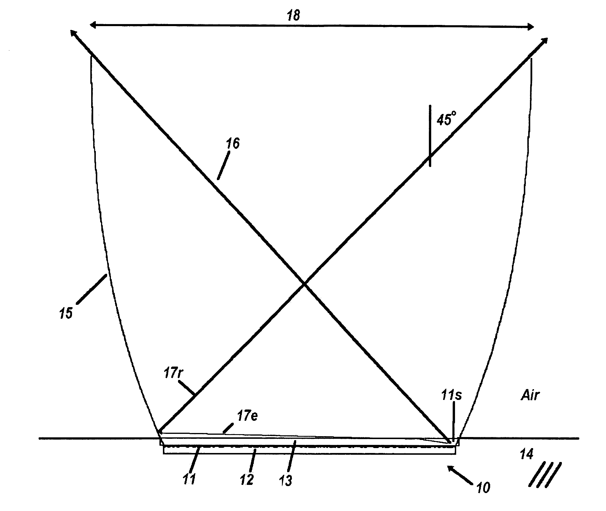
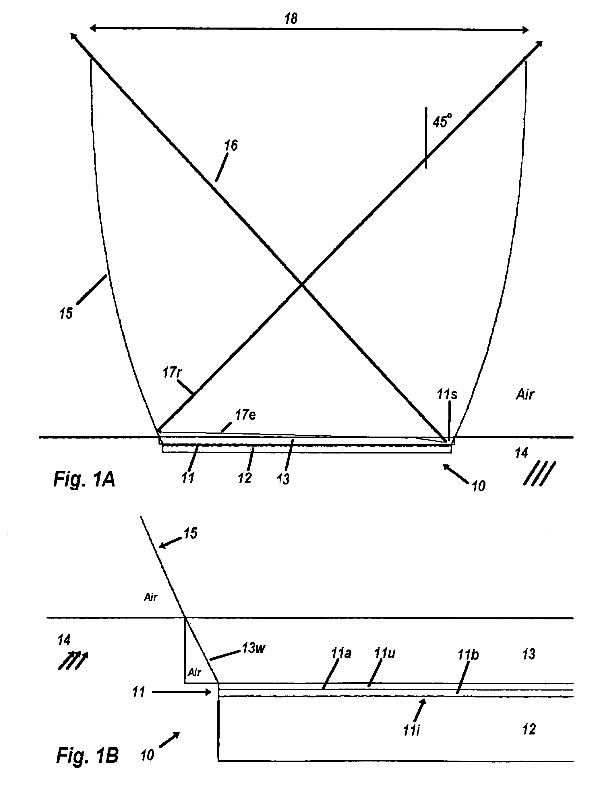
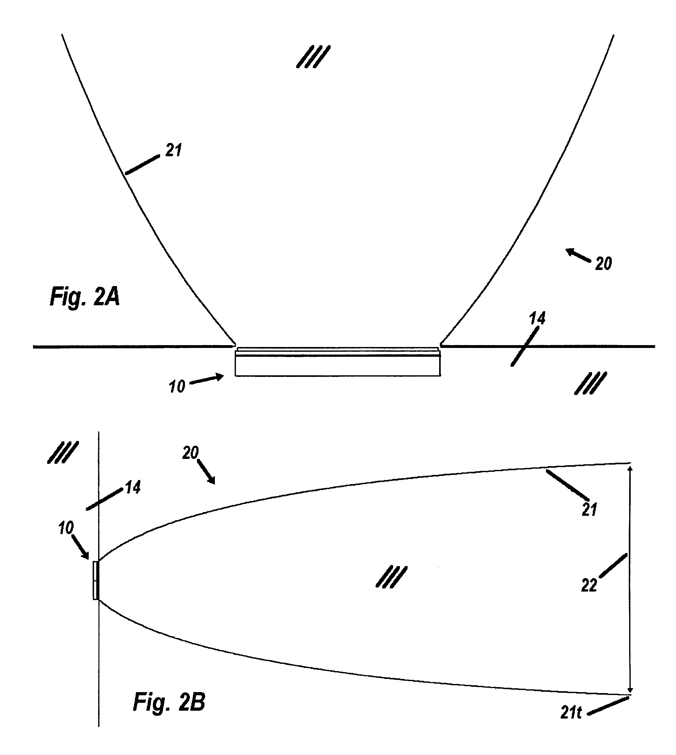
[0187]

anglea device that delivers luminance from one plane to anotherrotatorlying at a tilt to the firstCECcompound elliptical concentratorCPCcompound parabolic concentratorcross-CPCa three-dimensional (3-D) configuration having a 2-D CPCprofile in two orthogonal directionsdichroica filter that has two distinct transmission peaksfilterdome ofan approximately spherical LED cover made of transparentLEDdielectric materialsedge-raythe foundational principle of non-imaging optics, whereby aprincipledefining set of rays from the edge of an aperture areguaranteed to be delivered to the edge of another aperture,but the first aperture is not imaged onto the secondetenduethe optical manifestation of entropy, defined as the...


PUM


Abstract

An optical manifold for efficiently combining a plurality of blue LED outputs to illuminate a phosphor for a single, substantially homogeneous output, in a small, cost-effective package. Embodiments are disclosed that use a single or multiple LEDs and a remote phosphor, and an intermediate wavelength-selective filter arranged so that backscattered photoluminescence is recycled to boost the luminance and flux of the output aperture. A further aperture mask is used to boost phosphor luminance with only modest loss of luminosity. Alternative non-recycling embodiments provide blue and yellow light in collimated beams, either separately or combined into white.

Description

CROSS REFERENCE TO RELATED APPLICATIONS[0001]This application is a continuation-in-part of U.S. patent application Ser. No. 11 / 115,055 for “OPTICAL MANIFOLD FOR LIGHT-EMITTING DIODES” of Chaves et al. filed Apr. 25, 2005, now U.S. Pat. No. 7,286,296, the disclosure of which is incorporated herein by reference in its entirety.[0002]Application Ser. No. 11 / 115,055 claims the benefit of U.S. Provisional Patent Application No. 60 / 658,713, filed Mar. 3, 2005, entitled OPTICAL MANIFOLDS FOR LIGHT-EMITTING DIODES, which is incorporated by reference herein in its entirety.[0003]Application Ser. No. 11 / 115,055 claims the benefit of U.S. Provisional Patent Application No. 60 / 614,565, filed Sep. 29, 2004, entitled OPTICAL MANIFOLDS FOR LIGHT-EMITTING DIODES, which is incorporated by reference herein in its entirety.[0004]Application Ser. No. 11 / 115,055 claims the benefit of U.S. Provisional Patent Application No. 60 / 612,558, filed Sep. 22, 2004, entitled OPTICAL MANIFOLDS FOR LIGHT-EMITTING DI...

Claims


Application Information

Patent Timeline
Patent Type & Authority Patents(United States)
IPC IPC(8): F21V9/00F21K99/00F21V8/00H01L33/58H01L33/60
CPCF21K9/00G02B6/0018G02B6/0028G02B6/0046G02B6/0068G02B6/0073G02B27/0905G02B27/095G02B27/0983G02B27/1066G02B27/123G02B27/126G02B27/149F21K9/52H01L2924/0002F21V7/0091F21Y2101/02G02B3/08H01L33/58H01L33/60H01L2924/00F21K9/61F21Y2113/10F21Y2115/10F21S41/141F21S41/18F21S41/285F21S41/24F21S45/47F21S41/16F21S41/176
Inventor CHAVES, JULIO C.FALICOFF, WAQIDIMINANO, JUAN C.BENITEZ, PABLOPARKYN, JR., WILLIAM A.ALVAREZ, ROBERTODROSS, OLIVER
Owner SEOUL SEMICONDUCTOR
Why Eureka
Try Eureka