Method for fabricating semiconductor device and display device

a technology of display device and semiconductor, applied in the direction of liquid/solution decomposition chemical coating, superimposed coating process, instruments, etc., can solve the problems of increasing cost, reducing yield, and inability to meet users' needs, so as to reduce defects and reduce unevenness.

Inactive Publication Date: 2008-06-10
SEMICON ENERGY LAB CO LTD
View PDF30 Cites 17 Cited by
  • Summary
  • Abstract
  • Description
  • Claims
  • Application Information

AI Technical Summary

Benefits of technology

[0014]In view of the above problems, it is an object of the present invention to alleviate unevenness due to the contact hole 102 for forming a contact with the conductive film 100 in the lower layer even when the contact hole 102 has a large diameter (1 μm or more). Thus, it is a further object of the invention to reduce defects caused by the unevenness due to the contact hole 102.
[0015]It is a feature of the invention to form a wiring after a contact hole is filled with conductive fine particles. The conductive fine particles can be easily dispersed into a wiring material by using conductive fine particles having high wettability with the wiring material, thereby making a contact. Thus, planarization of a contact hole can be achieved without performing a reflow process. When the reflow process is not performed, reliability of around a contact hole can be improved in relatively advantageous condition to energy cost. Further, in the invention, a depression reflecting the shape of the contact hole may be filled with the conductive fine particles 103 after forming a wiring.
[0016]In the case where a reflow process is performed, the conductive fine particles may use a material which dissolves at lower temperatures, or a material which is alloyed with the wiring material at lower temperatures. Thus, a contact hole can easily be planarized by a reflow process at lower temperatures. In this case, connection with higher reliability can be obtained since the wiring material and the conductive fine particles are combined or alloyed.
[0017]The planarization is enabled, and a large step height can be inhibited by applying the invention. Thus, the invention can significantly contribute to improvements in yield and reliability of a semiconductor device, or the like.
[0018]A wiring is formed after a contact hole is filled with conductive fine particles, and the conductive fine particles use a material having high wettability with the wiring material. Thus, planarization of a contact hole can be achieved without performing a reflow process. When the reflow process is not performed, reliability of around a contact hole can be improved in relatively advantageous condition to energy cost.
[0019]In the case where a reflow process is performed, the conductive fine particles may use a material which dissolves at lower temperatures, or a material which is alloyed with the wiring material at lower temperatures. Thus, a contact hole can easily be planarized by a reflow process at lower temperatures. In this case, connection with higher reliability can be obtained since the wiring material and the conductive fine particles are combined or alloyed.

Problems solved by technology

How to produce advanced electronic devices without increasing the cost becomes key; however, if reliability and quality are sacrificed, it is impossible to satisfy users' needs.
Defects in the devices using semiconductor elements are some of the factors to cause lower yield.
When forming a conductive film used for a wiring, disconnection and high resistivity of the wiring is occasionally caused by poor coverage of the conductive film.
The poor coverage mostly occurs around an opening where the conductive film makes a contact with the lower layer.
Further, the poor coverage can occur, for example, when the contact is not made since the opening is not covered with a wiring material, or when a part of a wiring becomes too thin.
Display defects and unevenness are often due to unevenness caused reflecting the shape of the opening for forming a contact with the lower layer or the shape of the conductive film in the lower layer.
When the unevenness leads to nonuniformly of the electrical field, display unevenness are caused in a liquid crystal display device.
Meanwhile in an EL device, display defects such as dark spots and bright spots would be caused as well as display unevenness.
Such a step may cause further reduction in yield.
In order to prevent such high resistance and disconnection, an approach to increase the thickness of the wiring 104 can be conceived; however, excessive thickness is undesirable in view of integration.
Accordingly, even a countermeasure such as etchback as in Reference 1 is taken, the accuracy of the etchback would cause a problem.

Method used


Image

  • Method for fabricating semiconductor device and display device
  • Method for fabricating semiconductor device and display device
  • Method for fabricating semiconductor device and display device

Examples


embodiment mode 1

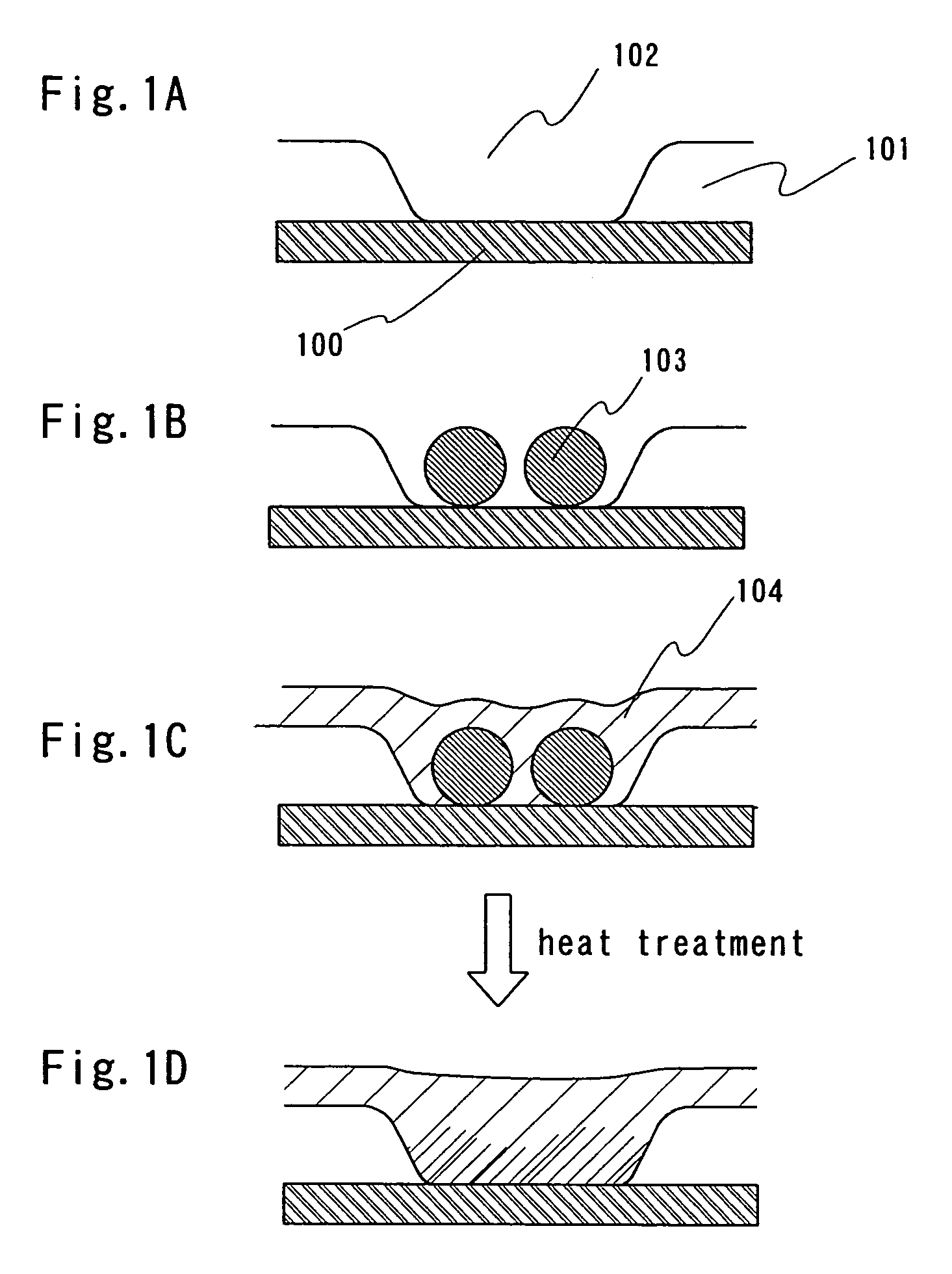
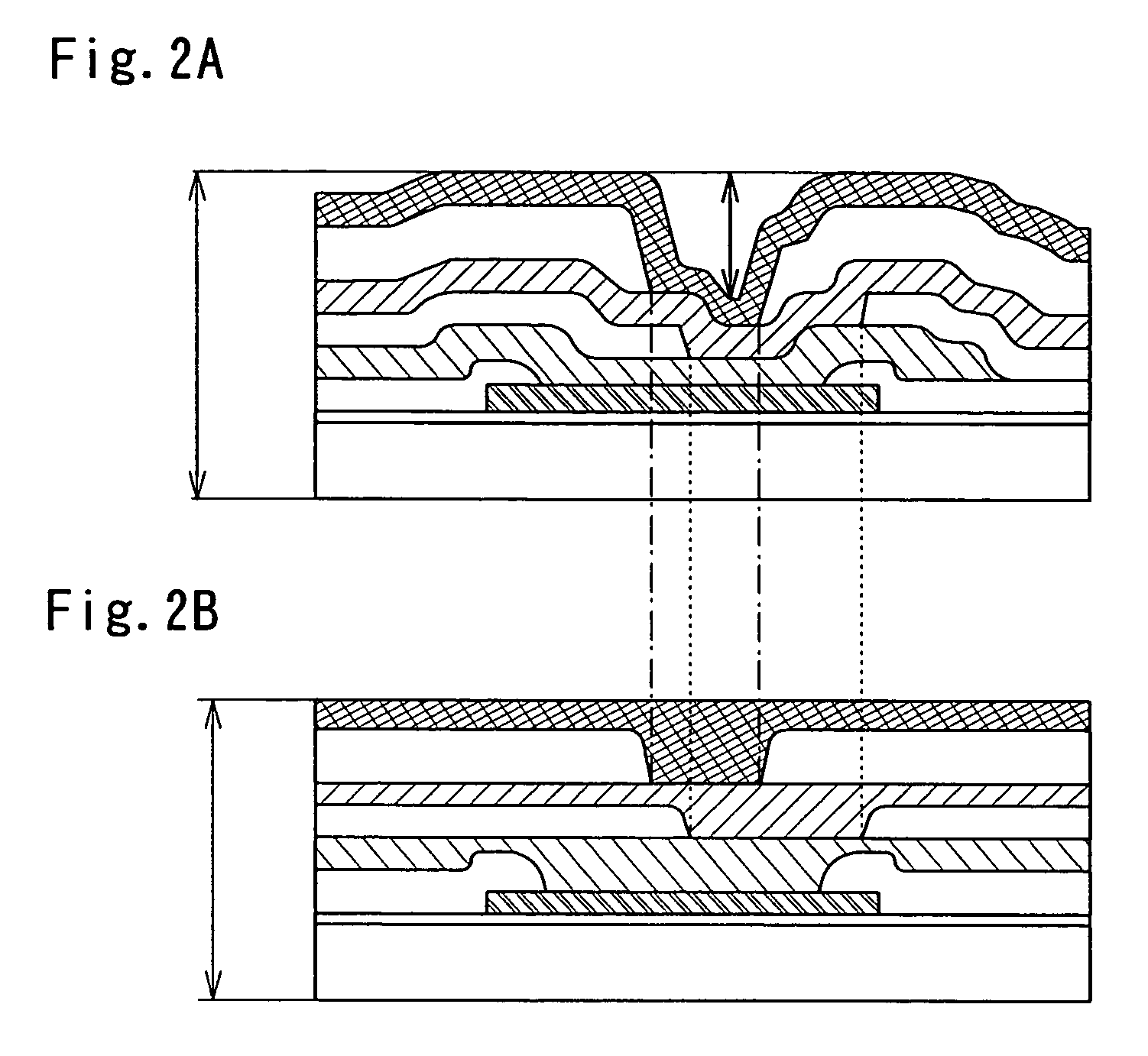
[0038]An embodiment mode of the invention will be described with reference to FIGS. 1A to 2B.

[0039]In FIGS. 1A to 1D, a contact hole 102 is formed in an insulating film 101 (FIG. 1A), and the wiring 104 is formed over the insulating film 101 over a conductive layer 100 on a surface. Thus, the wiring 104 is connected to the conductive layer 100 through the contact hole 102.

[0040]Next, a contact hole 102 is filled with conductive fine particles 103 (FIG. 1B). Material which has high wettability with a material of a wiring 104 may be used for the conductive fine particles 103.

[0041]Next, a wiring 104 is formed so as to cover at least the conductive fine particles 103 and a part of the contact hole 102 (FIG. 1C). Since the conductive fine particles 103 uses material having high wettability with a material of the wiring 104, the conductive fine particles 103 can be easily dispersed in the wiring material, and a contact can be made. Thus, planarization of the contact hole can be realized ...

embodiment mode 2

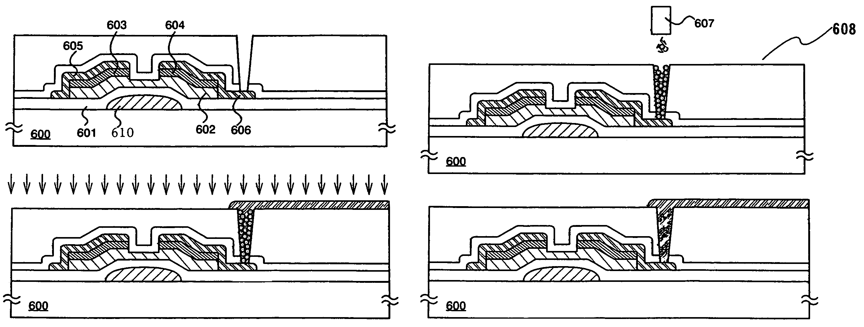
[0044]An embodiment mode of the invention will be described with reference to FIGS. 5A to 5D. In this embodiment mode, a contact hole 102 can be selectively filled with a dispersion liquid 108 containing the conductive fine particles 103 by employing droplet discharging method, thereby obtaining planarity.

[0045]The droplet discharging method is commonly referred to as an ink-jet method. In the technology, droplets of a solution to be applied are discharged from a nozzle 107 and applied to a certain area. In the invention, the technology is applied using a special ink in which the conductive fine particles 103 are dispersed.

[0046]The contact hole 102 formed in the insulating film 101 is filled with the dispersion liquid 108 containing the conductive fine particles 103 discharged from the nozzle 107 of a drop discharging device so that the wiring 104 can be electrically connected to the conductive layer 100 in the lower layer.

[0047]The filling of the contact hole by droplet dischargin...

embodiment mode 3

[0056]Another embodiment mode of the invention will be described with reference to FIGS. 7A to 7E. A dispersion liquid 108 of conductive fine particles 103 is applied all over the insulating film where a contact hole 102 is formed by an application method such as spin coating so as to be connected to a conductive layer 100. Next, a material having a shape which does not damage the substrate surface, such as a silicon resin plate (in this embodiment mode, a spatula 111 of silicon resin is used) is pushed to the substrate surface and moved so as to fill the contact hole 102 with the applied dispersion liquid 108 containing the conductive fine particles 103. Concurrently, the dispersion liquid 108 containing the conductive fine particles 103 adhered to an undesired portion is removed. Thus, only inside the contact hole 102 can be selectively filled with the dispersion liquid 108 containing the conductive fine particles 103.

[0057]Other than by spin coating, the contact hole can also be ...


PUM

PropertyMeasurementUnit
diameteraaaaaaaaaa
evaporating temperatureaaaaaaaaaa
melting pointaaaaaaaaaa

Abstract

It is an object of the present invention to alleviate unevenness due to an opening for making a contact with the lower layer even when the opening has a large diameter (1 μm or more). Thus, it is a further object of the invention to reduce defects caused by the unevenness due to the contact hole. It is a feature of the invention to form a wiring by filling the contact hole with conductive fine particles. The conductive fine particles can be easily dispersed into a wiring material by using conductive fine particles having high wettability with the wiring material, thereby making a contact. Thus, planarization of a contact hole can be achieved without performing a reflow process. Further, more planarity can be obtained by performing a reflow process in addition, and the reliability is improved accordingly.

Description

BACKGROUND OF THE INVENTION[0001]1. Field of the Invention[0002]The present invention relates to a method for fabricating a semiconductor device. More specifically, the invention relates to a method for forming a contact between wirings of a semiconductor device.[0003]2. Description of the Related Art[0004]In recent years, in accordance with the development of technology, miniaturization and performance of electronic devices has been advanced, and the highly developed electronic devices are everywhere. In order to maintain a company's competitive edge, it has become very important not only to produce better products than other companies, but also to offer such products at lower prices.[0005]How to produce advanced electronic devices without increasing the cost becomes key; however, if reliability and quality are sacrificed, it is impossible to satisfy users' needs. Higher production yields is a very effective measure to achieve further price reduction without degrading performance, ...

Claims


Application Information

Patent Timeline
Patent Type & Authority Patents(United States)
IPC IPC(8): H01L21/44G02F1/1362H01L21/288H01L21/768H01L21/77H01L21/84
CPCH01L21/288H01L27/1292H01L21/76877H01L21/76882H01L21/7684G02F1/136227
Inventor YAMAZAKI, SHUNPEI
Owner SEMICON ENERGY LAB CO LTD
Why Eureka
Try Eureka