Method of driving light emitting element array

a technology of light emitting elements and arrays, which is applied in the direction of process and machine control, optical radiation measurement, instruments, etc., can solve the problems of poor rise-up characteristics, long time for light emitting elements, poor stability, etc., and achieve excellent rise-up characteristics, high stability, and excellent response.

Active Publication Date: 2008-06-10
UDC IRELAND +1
View PDF13 Cites 7 Cited by
  • Summary
  • Abstract
  • Description
  • Claims
  • Application Information

AI Technical Summary

Benefits of technology

[0014]In view of the foregoing observations and description, the primary object of the present invention is to provide a method of driving a light emitting element array forming an exposure system which can realize excellent rise-up characteristics and suppress fluctuation in response and / or light emission of the light emitting elements.
[0021]In the method of the present invention, since the light emitting elements are driven in the constant-voltage drive at least during beginning of the subsequent exposure periods, excellent rise-up characteristics can be obtained by virtue of the fact that the constant-voltage drive is excellent in response. Further, since the voltage applied to each of the light emitting elements during the constant-voltage drive is equal to the anode voltage when the light emitting element is driven is the constant-current drive, a constant current is supplied to the light emitting element and accordingly, fluctuation in response and / or light emission of the light emitting elements due to change with time of the environment of use or each light emitting element can be suppressed, whereby high stability can be realized.
[0022]When the light emitting elements are driven in the constant-voltage drive only for a predetermined period during the beginning of the exposure period and in the constant-current drive in the exposure period after the predetermined period, the operation of the light emitting element array can be more stabilized. The current-voltage characteristic of the light emitting element can be changed before completion of exposure of one image due to the self-heat generation of the element. However, by driving the light emitting element in the constant-current drive in the exposure period after the predetermined period, the light emission can be prevented from being fluctuated in the exposure period due to the error in the current by the change of the current-voltage characteristic of the light emitting element.
[0023]The current-voltage characteristic of the light emitting element can be changed after the anode voltage is measured and before the image exposure is initiated. When the light emitting elements are driven by a signal pulse-width-modulated according to the image data with the pulse width defined by the number of clocks, by driving the light emitting elements in the constant-voltage drive for a very short time interval defined by one clock pulse from the time point at which the light emission is initiated, the light emission can be prevented from being fluctuated in the exposure period due to the error in the current by the change of the current-voltage characteristic of the light emitting element after the very short time interval, whereby adverse influence on the quality of the exposed image can be minimized.
[0024]Generally, the rise-up time of the organic EL element is substantially equal to the very short time interval defined by one clock pulse, the result of improving the rise-up characteristics is remarkable even if the light emitting elements is driven in the constant-voltage drive for the very short time interval.
[0025]Further, though the steps of driving the light emitting elements in constant-current drive, and measuring the anode voltage of each light emitting element at that time can be executed before and / or during an exposure period, it is preferred from the view point of improving the quality of the exposed image to execute before the exposure period in that fluctuation of the light emission can be prevented over the entire exposure period. Whereas it is preferred from the view point of making higher the exposure processing speed to execute during the exposure period in that the time for the steps need not be additionally provided.

Problems solved by technology

The former is excellent in response but is poor in stability due to drop and fluctuation of the forward voltage by change with time of the environment of use or each light emitting element.
However, when the constant-current drive system is employed for the light emitting element array of the simple matrix system, there has been known a problem that the rise-up characteristics are bad.
However due to existence of the parasitic capacity described above, all capacities of the light emitting elements formed on the anode are charged with the constant current when the scanning electrodes are switched and accordingly, it requires a long time for the light emitting element to emit light after its capacity is charged, which deteriorates the rise-up characteristics.
However the anode voltage of each light emitting element upon the constant-current drive is not always constant and the anode voltages of the light emitting elements in one array fluctuate according to the initial difference and / or the change with time of the light emitting elements.
Such fluctuation and / or difference of the anode voltage lead to fluctuation of the rise-up time.
Though the fluctuation in the light emission does not give rise to a significant problem when the light emitting element array is used as a display means, the fluctuation in the light emission causes deterioration of the quality the exposed image when the light emitting element array is used as an exposure head.
Especially, the difference in the light emission between the elements causes a scoring unevenness extending in a sub-scanning direction to greatly deteriorate the quality of the exposed image when the exposure head and the photosensitive material are moved in the sub-scanning direction (sub-scanning).

Method used


Image

  • Method of driving light emitting element array
  • Method of driving light emitting element array
  • Method of driving light emitting element array

Examples


Embodiment Construction

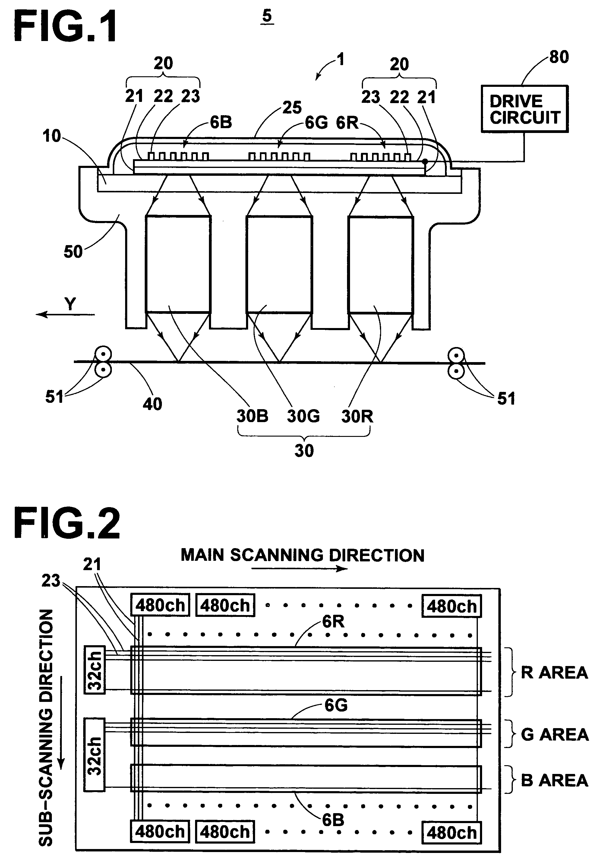
[0038]As shown in FIG. 1, an exposure system 5 in accordance with an embodiment of the present invention has an exposure head 1. The exposure head 1 comprises a transparent base 10, a number of organic EL elements 20 formed on the base 10 by deposition, a refractive index profile type lens array 30 (30R, 30G and 30B) which is a unit system for imaging on a color photosensitive sheet 40 an image generated by the light emitted from the organic EL elements 20, and a support 50 which supports the base 10 and the refractive index profile type lens array 30.

[0039]The exposure system 5 further comprises, in addition to the exposure head 1, a sub-scanning means 51 in the form of, for instance, a pair of nip rollers which conveys the color photosensitive sheet 40 at a constant speed in a direction of arrow Y.

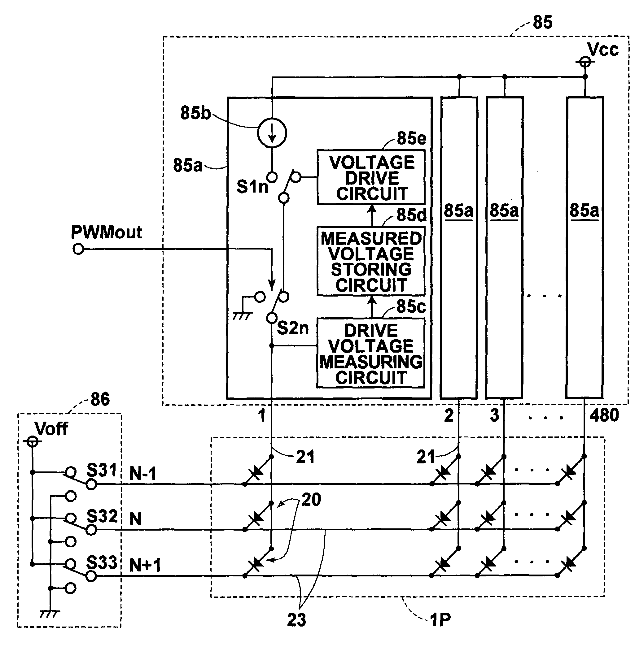
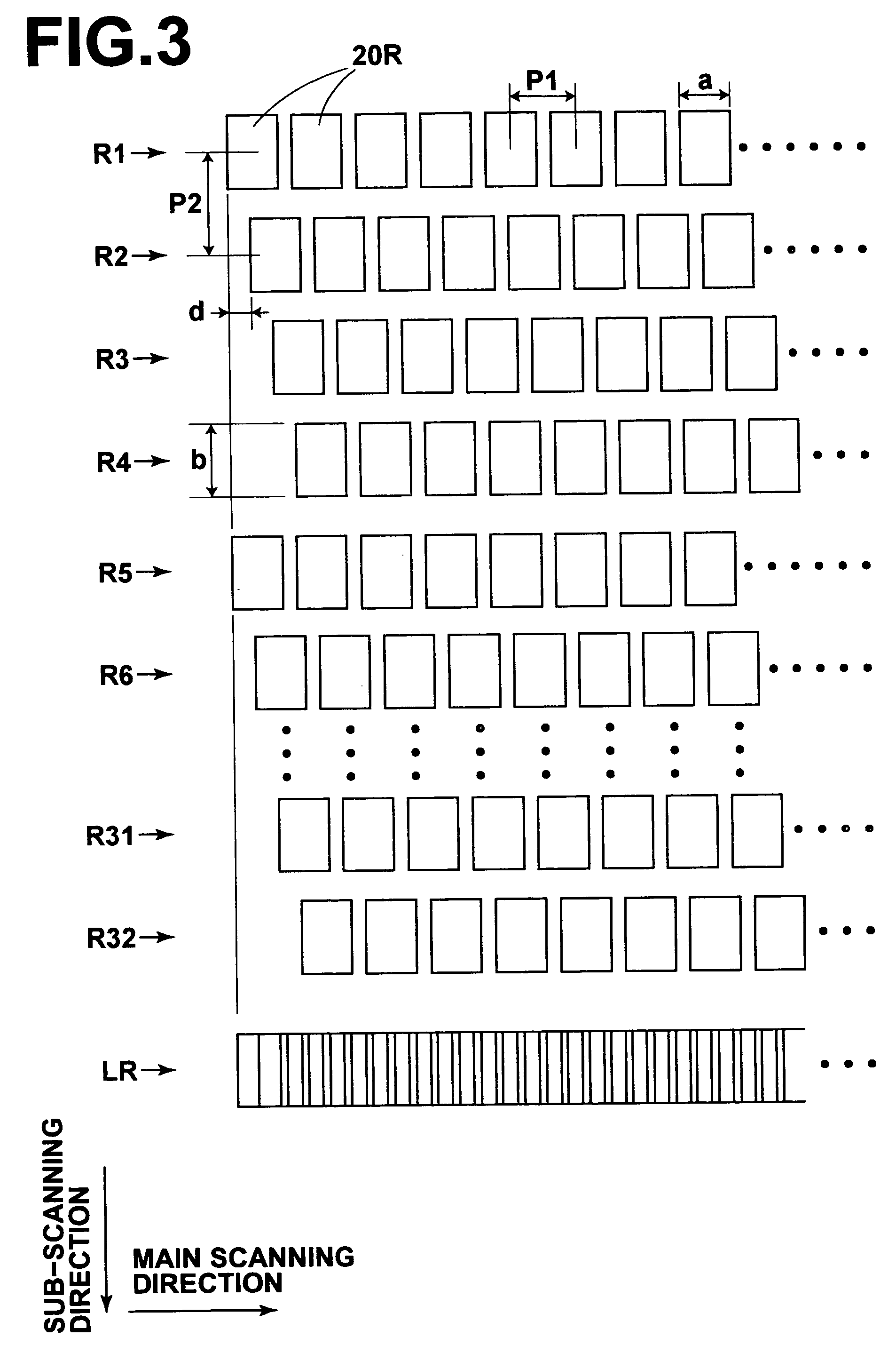
[0040]The organic EL elements 20 comprises a transparent anode 21, an organic compound layer 22 including a light emitting layer and patterned for each pixel and a metal cathode 23 forme...


PUM


Abstract

An exposure system is provided with a light emitting element array formed by a plurality of light emitting elements formed at the intersections of anodes and cathodes arranged in matrix so that a photosensitive material is exposed to an image formed on the light emitting element array. A method of driving the light emitting element array includes the steps of driving the light emitting elements in constant-current drive before and / or during an exposure period, measuring and storing in a memory means the anode voltage of each light emitting element at that time, and driving the light emitting elements in constant-voltage drive at a voltage equal to the measured anode voltage at least during beginning of the subsequent exposure periods.

Description

BACKGROUND OF THE INVENTION[0001]1. Field of the Invention[0002]This invention relates to a method of driving a light emitting element array such as an organic EL (electroluminescent) element array.[0003]2. Description of the Related Art[0004]Conventionally, there has been known an exposure system which comprises a light emitting element array comprising a plurality of two-dimensionally arranged light emitting elements, such as organic EL elements, and a drive circuit which controls the light emitting time (light emitting pulse width) of each of the light emitting elements on the basis of an image data carrying thereon a gradation image and exposes a photosensitive material to an image formed on the light emitting element array on the basis of the image data. An example of such an exposure system is disclosed in U.S. patent Laid-Open No. 20010052926.[0005]As a representative of the light emitting element array, there have been known those of a system so-called a simple matrix system...

Claims


Application Information

Patent Timeline
Patent Type & Authority Patents(United States)
IPC IPC(8): G09G3/32B41J2/44B41J2/45B41J2/455G09G3/10G09G3/20G09G3/30H01L51/50H05B33/14
CPCG09G3/3216G09G3/2014G09G2300/0465G09G2320/0295
Inventor SETO, YASUHIRO
Owner UDC IRELAND
Why Eureka
Try Eureka