Smart cache

Inactive Publication Date: 2008-06-10
TEXAS INSTR INC
View PDF15 Cites 0 Cited by
  • Summary
  • Abstract
  • Description
  • Claims
  • Application Information

AI Technical Summary

Benefits of technology

[0012]The present invention provides significant advantages over the prior art. First, the RAM set cache (mapped to a contiguous block of main memory addresses) can significantly improve the operation of a processing device performing real-time operations, since a desired block of code can be stored in the RAM set cache for fast retrieval. Second, there is no extra penalty for accessing a larger data memory for a RAM set cache, as long as the access time of the RAM set is not bigger than the access time of the standard cache. Third, the addition of one or more RAM set caches can be provided with a minimal amount of circuitry over a conventional cache. Fourth, the RA

Problems solved by technology

The main memory is generally much larger than the cache, but also significantly slower.
In most cases, however, increasing cache size has diminishing returns after a certain point.
Further, increasing the cache size will increase the size of the chip (assuming the cache is integrated with the processing core).
Accordingly, merely increasing the size of a cache will in many cases not produce worthwhile results.
In many devices, certain routines will have critical time constraints or will otherwise need a predictable execution time.
This mechanism is useful for entries that will be used repeatedly; however, locking entries of a cache reduces the size and

Method used


Image

  • Smart cache
  • Smart cache
  • Smart cache

Examples


Example

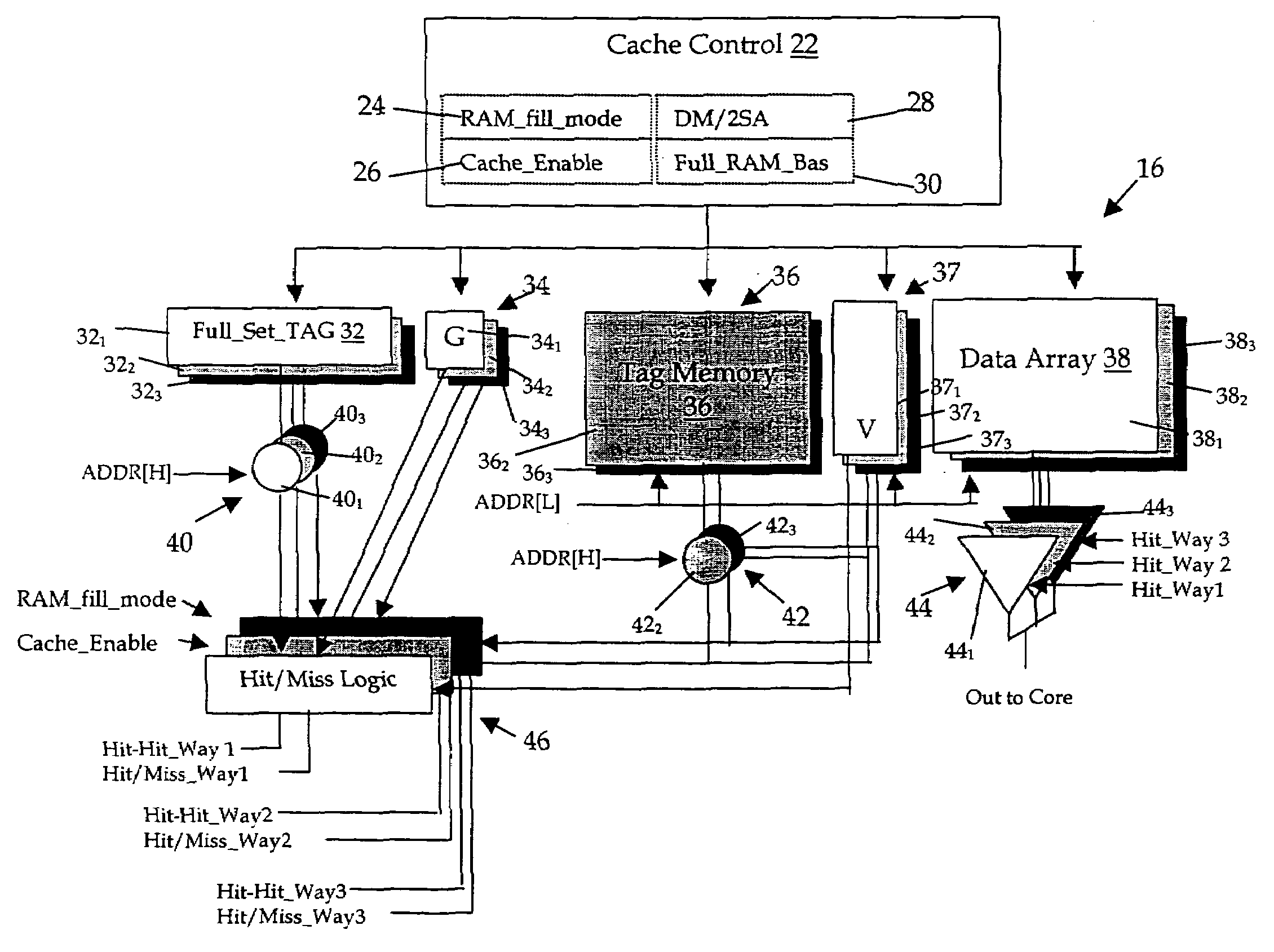
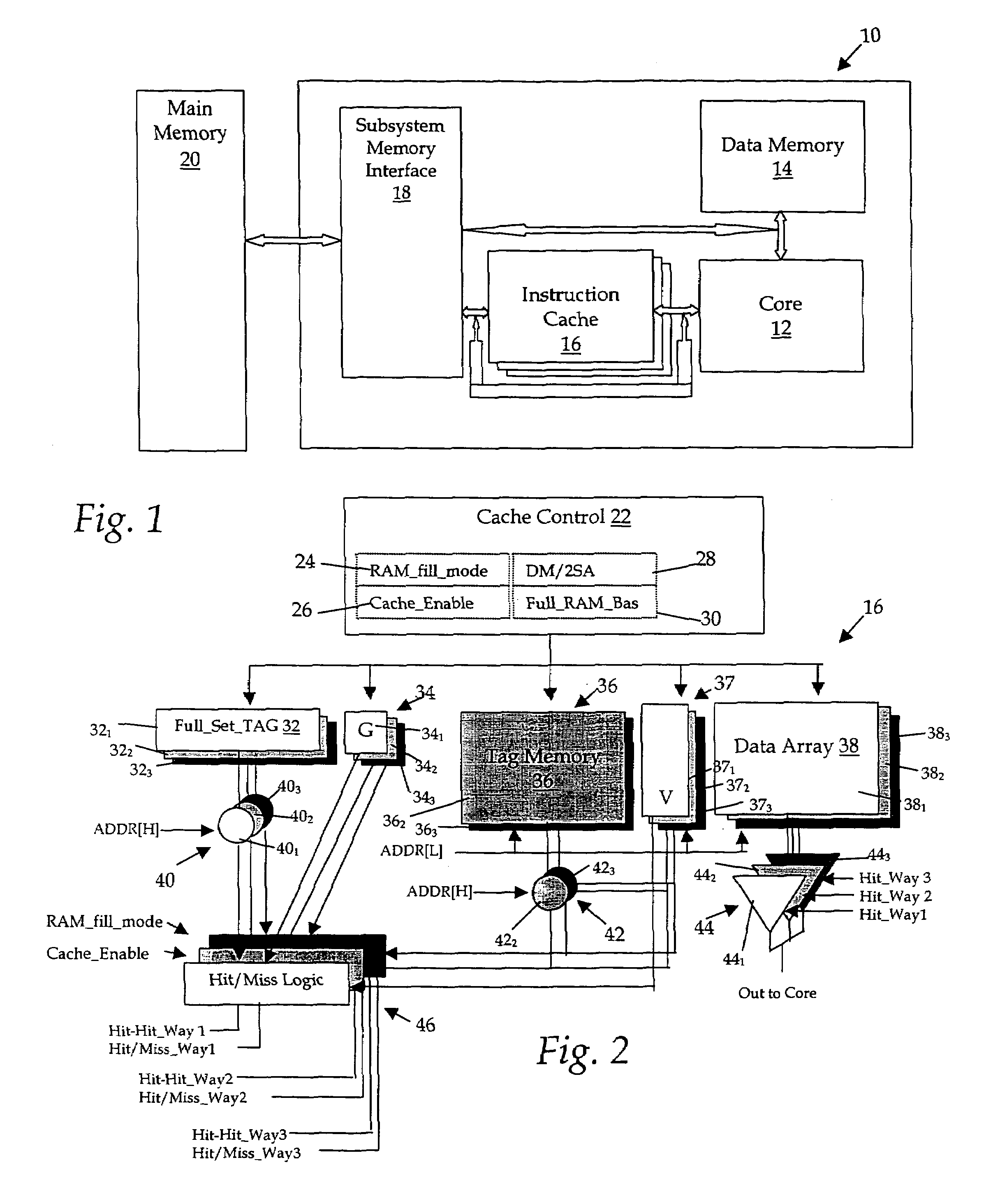
[0018]The present invention is best understood in relation to FIGS. 1-4 of the drawings, like numerals being used for like elements of the various drawings.

[0019]FIG. 1 illustrates a block diagram of a processing device 10. Processing device 10 includes a processing core 12, data memory 14, instruction cache 16, and subsystem memory interface 18. Subsystem memory interface 18 interfaces with main memory 20, which is typically an external memory.

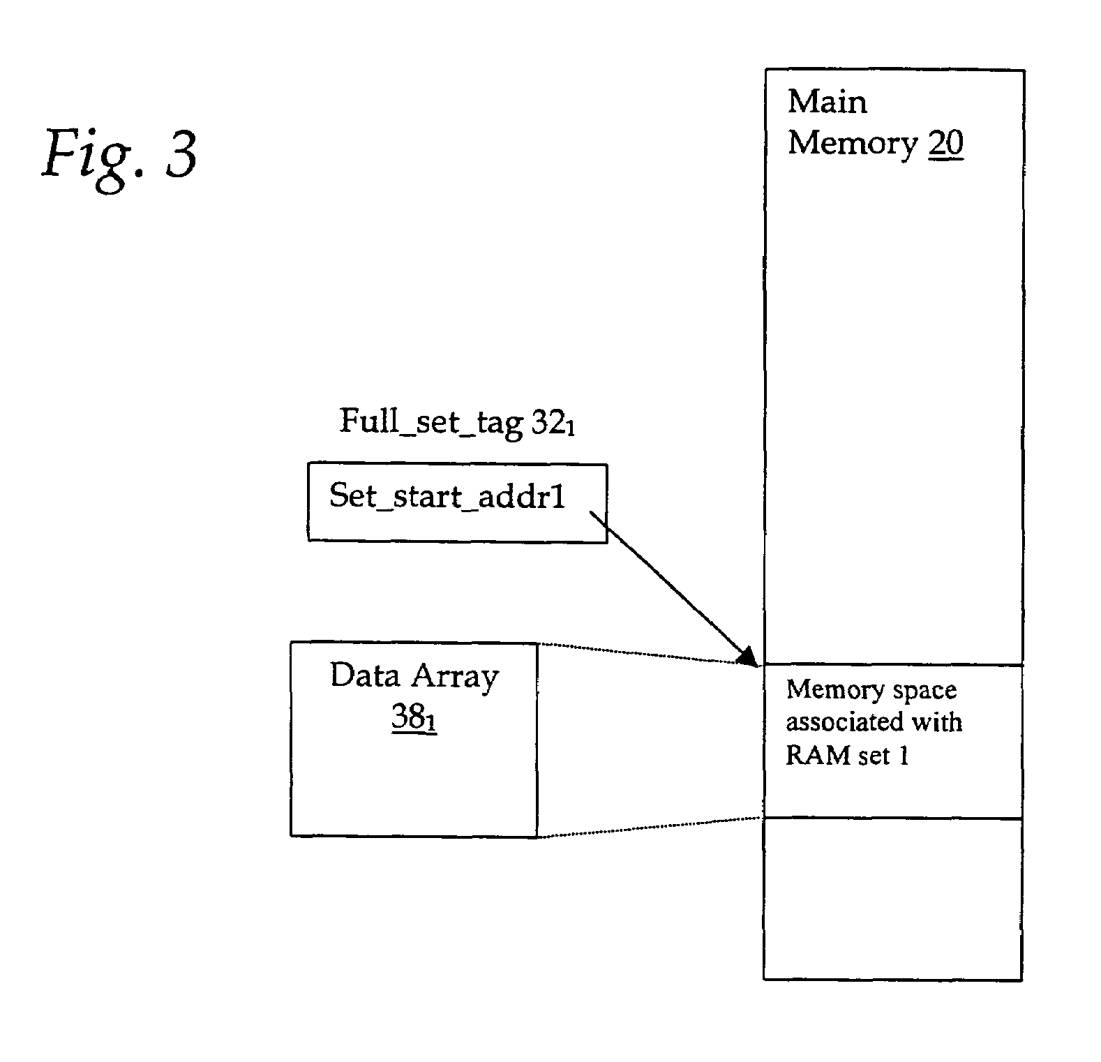
[0020]As described in greater detail below, in the preferred embodiment, the instruction cache is a 3-way cache with one cache way being a “RAM set” cache memory. The RAM set cache is designed to cache a contiguous block of memory starting from a chosen main memory address location. The other two cache ways can be configured as RAM set cache memories, or use another architecture. For example, the instruction cache 16 could be configured as one RAM set cache and a 2-way set associative cache.

[0021]In operation, the processing core 12 accesses ...


PUM


Abstract

A cache architecture (16) for use in a processing device includes a RAM set cache for caching a contiguous block of main memory (20). The RAM set cache can be used in conjunction with other cache types, such as a set associative cache or a direct mapped cache. A register (32) defines a starting address for the contiguous block of main memory (20). The data array (38) associated with the RAM set may be filled on a line-by-line basis, as lines are requested by the processing core, or on a set-fill basis which fills the data array (38) when the starting address is loaded into the register (32). As addresses are received from the processing core, hit/miss logic (46) the starting address register (32), a global valid bit (34), line valid bits (37) and control bits (24, 26) are used to determine whether the data is present in the RAM set or whether the data must be loaded from main memory (20). The hit/miss logic (46) also determines whether a line should be loaded into the RAM set data array (38) or in the associated cache.

Description

CROSS-REFERENCE TO RELATED APPLICATIONS[0001]Not ApplicableSTATEMENT OF FEDERALLY SPONSORED RESEARCH OR DEVELOPMENT[0002]Not ApplicableBACKGROUND OF THE INVENTION[0003]1. Technical Field[0004]This invention relates in general to processing devices and, more particularly, to a cache architecture for a processing device.[0005]2. Description of the Related Art[0006]Most processing devices use a cache architecture to increase the speed of retrieving information from a main memory. A cache memory is a high speed memory that is situated between the processing core of a processing device and the main memory. The main memory is generally much larger than the cache, but also significantly slower. Each time the processing core requests information from the main memory, the cache controller checks the cache memory to determine whether the address being accessed is currently in the cache memory. If so, the information is retrieved from the faster cache memory instead of the slower main memory. ...

Claims


Application Information

Patent Timeline
IPC IPC(8): G06F12/00G06F12/08
CPCG06F12/0848G06F12/0864
Inventor CHAUVEL, GERARDLASSERRE, SERGED'INVERNO, DOMINIQUE BENOIT JACQUES
Owner TEXAS INSTR INC
Why Eureka
Try Eureka