Method and apparatus for inspecting pattern defects

a pattern defect and pattern technology, applied in the field of inspection, can solve the problems of large image information obtained from an inspection target, insufficient consideration of requirements by the aforementioned conventional technology, and false information that should not be detected originally as a defect, and achieve the effect of high sensitivity and high speed

Inactive Publication Date: 2008-06-17
HITACHI HIGH-TECH CORP
View PDF23 Cites 134 Cited by
  • Summary
  • Abstract
  • Description
  • Claims
  • Application Information

AI Technical Summary

Benefits of technology

[0006]The present invention provides a pattern defect inspection method and apparatus that can reveal ultramicroscopic defects on an inspection target in which ultramicroscopic circuit patterns are formed, and can inspect the defects with high sensitivity and at a high speed.
[0020]The present invention makes it possible to reveal ultramicroscopic defects on an inspection target in which ultramicroscopic circuit patterns are formed, and inspect the defects with high sensitivity and at a high speed.
[0021]Further, the present invention makes it possible to attain an inspection speed that corresponds to the processing speed, which is determined, for instance, by the image sensor's image acquisition rate, image accumulation time, and scanning width.

Problems solved by technology

Consequently, the image information obtained from an inspection target will become huge.
However, these requirements are not adequately considered by the aforementioned conventional technology.
This is a problem that a false-information that should not be detected originally as a defect will occur so much.
However, the use of such a false-information avoidance method decreases the sensitivity so that the ultramicroscopic defect 4d, which corresponds to a difference value smaller than the increased threshold value, cannot be detected.

Method used


Image

  • Method and apparatus for inspecting pattern defects
  • Method and apparatus for inspecting pattern defects
  • Method and apparatus for inspecting pattern defects

Examples


first embodiment

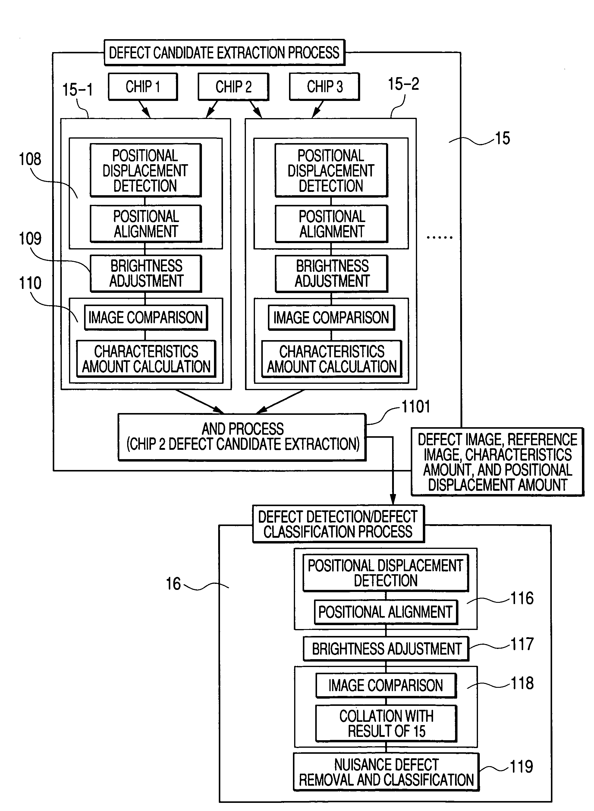
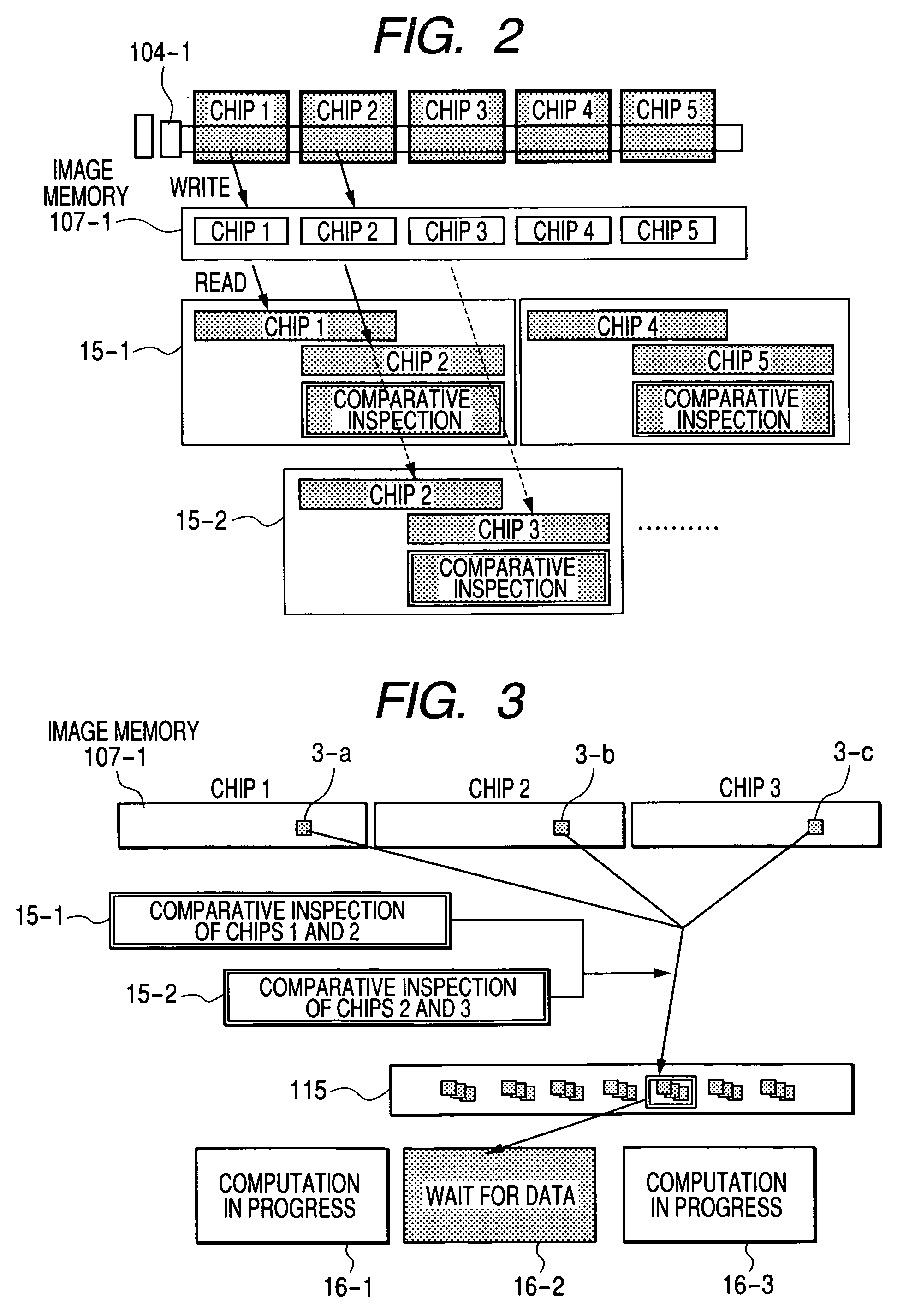
[0064]The defect candidate extraction unit 15 and defect detection unit 16 according to the present invention perform the process for extracting defect candidates from an acquired image and the process for detecting defects from a partial image containing defect candidates and classifying the detected defects. These processes are performed asynchronously with the process for detecting images from the image sensors and will now be described with references to FIGS. 2 and 3. It goes without saying that the process of the defect candidate extraction unit 15 may be performed asynchronously with the process of the defect detection unit 16. FIG. 2 illustrates a first embodiment and indicates how an image acquired by one image detection section (image sensor) 104-1 is processed. In the embodiment to be described, images sequentially acquired by the image detection section 104-1 and stored in the image memory 107-1 are processed in a parallel manner by two defect candidate extraction units ...

second embodiment

[0066]FIG. 3 illustrates a second embodiment and indicates image processing steps that are performed to detect defects from a partial image containing extracted defect candidates and classify the detected defects. The reference numeral 3-b in FIG. 3 denotes a partial image containing defect candidates that are extracted because their coordinates in units 15-1 and 15-2 agree with each other. The reference numerals 3-a and 3-c denote partial images that correspond to partial image 3-b. After partial image 3-b, either or both of partial images 3-a and 3-c, the amount of feature, and the amount of positional displacement are stored in memory 115, the defect detection unit 16 reads two partial images (3-b and 3-a or 3-b and 3-c) or three partial images (3-b, 3-a, and 3-c), the amount of feature, and the amount of positional displacement from memory 115 and performs a series of processing steps. The inspection apparatus according to the present invention includes three defect detection un...


PUM

PropertyMeasurementUnit
sizeaaaaaaaaaa
wavelengthaaaaaaaaaa
diametersaaaaaaaaaa

Abstract

The present invention relates to a pattern defect inspection method and apparatus that reveal ultramicroscopic defects on an inspection target in which ultramicroscopic circuit patterns are formed, and inspect the defects with high sensitivity and at a high speed. The present invention provides a pattern inspection apparatus for comparing the images of corresponding areas of two formed patterns that should be identical with each other, and judging any mismatched image area as a defect. The pattern inspection apparatus includes means for performing an image comparison process on a plurality of areas in a parallel manner. Further, the pattern inspection apparatus also includes means for converting the gradation of the image signals of compared images in each of a plurality of different processes. Therefore, the present invention can properly detect defects even if the same patterns of compared images differ in brightness.

Description

BACKGROUND OF THE INVENTION[0001]The present invention relates to an inspection technology for comparing between a detected image and a reference image of an inspection target, which is obtained through the use, for instance, of light or laser beam, and detecting microscopic pattern defects, foreign matter, and the like based on the differences, and more particularly to a pattern defect inspection method and apparatus that are suitable for conducting a visual inspection of semiconductor wafers, TFTs, photomasks, and the like.[0002]A known conventional technology for pattern defect inspection is disclosed, for instance, by Japanese Patent Laid-open No. 2001-5961.[0003]A microscopic defect inspection apparatus is disclosed by Japanese Patent Laid-open No. 2001-5961. This microscopic defect inspection apparatus includes an image signal detection section, an analog-to-digital conversion section, a delay circuit section, a first image processing circuit section, a second image processing...

Claims


Application Information

Patent Timeline
Patent Type & Authority Patents(United States)
IPC IPC(8): G06K9/00G01B11/30G01N21/95G01N21/956G06T1/00G06T7/00H01L21/66
CPCG01N21/9501G01N21/95607G06T7/001G06T2207/30148
Inventor SAKAI, KAORUMAEDA, SHUNJIOKABE, TAKAFUMI
Owner HITACHI HIGH-TECH CORP
Why Eureka
Try Eureka