Method of correcting mask pattern

a mask pattern and mask technology, applied in the field of mask pattern correction and mask pattern correction, can solve the problems of inability to accurately transfer the pattern, serious impact on the accuracy of the pattern and the process window, and the susceptibility of the pattern on the mask to the corner rounding effect, so as to achieve high accuracy and increase the reliability and throughput of production. , the effect of high accuracy

Active Publication Date: 2008-06-24
WINBOND ELECTRONICS CORP
View PDF8 Cites 2 Cited by
  • Summary
  • Abstract
  • Description
  • Claims
  • Application Information

AI Technical Summary

Benefits of technology

[0008]Accordingly, at least one objective of the present invention is to provide a method of correcting a mask pattern and a correcting apparatus thereof that can avoid the corner-rounding problem and produce a highly accurate pattern on the mask. In addition, the reliability and throughput of the production is increased.
[0018]In the present invention, a look-up table is built so that a corrective action can be implemented before forming a pattern on the mask. Hence, more accurate patterns are fabricated. In other words, the pattern is prevented from having corner rounding problem, thereby increasing the reliability and throughput of the fabrication process.

Problems solved by technology

If the pattern on the photomask is inaccurate, an inaccurate pattern will be transferred.
One disadvantage of the laser beam method is the susceptibility of the pattern on the mask to the corner rounding effect as shown in the distorted pattern 102 in FIG. 1.
The accuracy of the pattern and the process window are seriously affected especially when the dimension of the circuit design pattern is small.
However, using an electronic beam to write out the pattern has a throughput significantly lower than using a laser beam.
Furthermore, the cost of producing a mask using the electronic beam method is more than 5 times the cost of producing the same mask using the laser beam method.
However, the method in the disclosure limits the formation of the pattern on the mask through the selected mask writer.
Hence, the method can hardly solve the aforementioned problem.

Method used


Image

  • Method of correcting mask pattern
  • Method of correcting mask pattern
  • Method of correcting mask pattern

Examples


Embodiment Construction

[0026]Reference will now be made in detail to the present preferred embodiments of the invention, examples of which are illustrated in the accompanying drawings. Wherever possible, the same reference numbers are used in the drawings and the description to refer to the same or like parts.

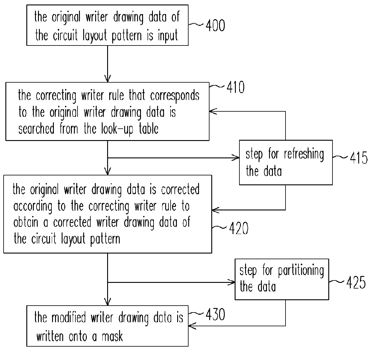
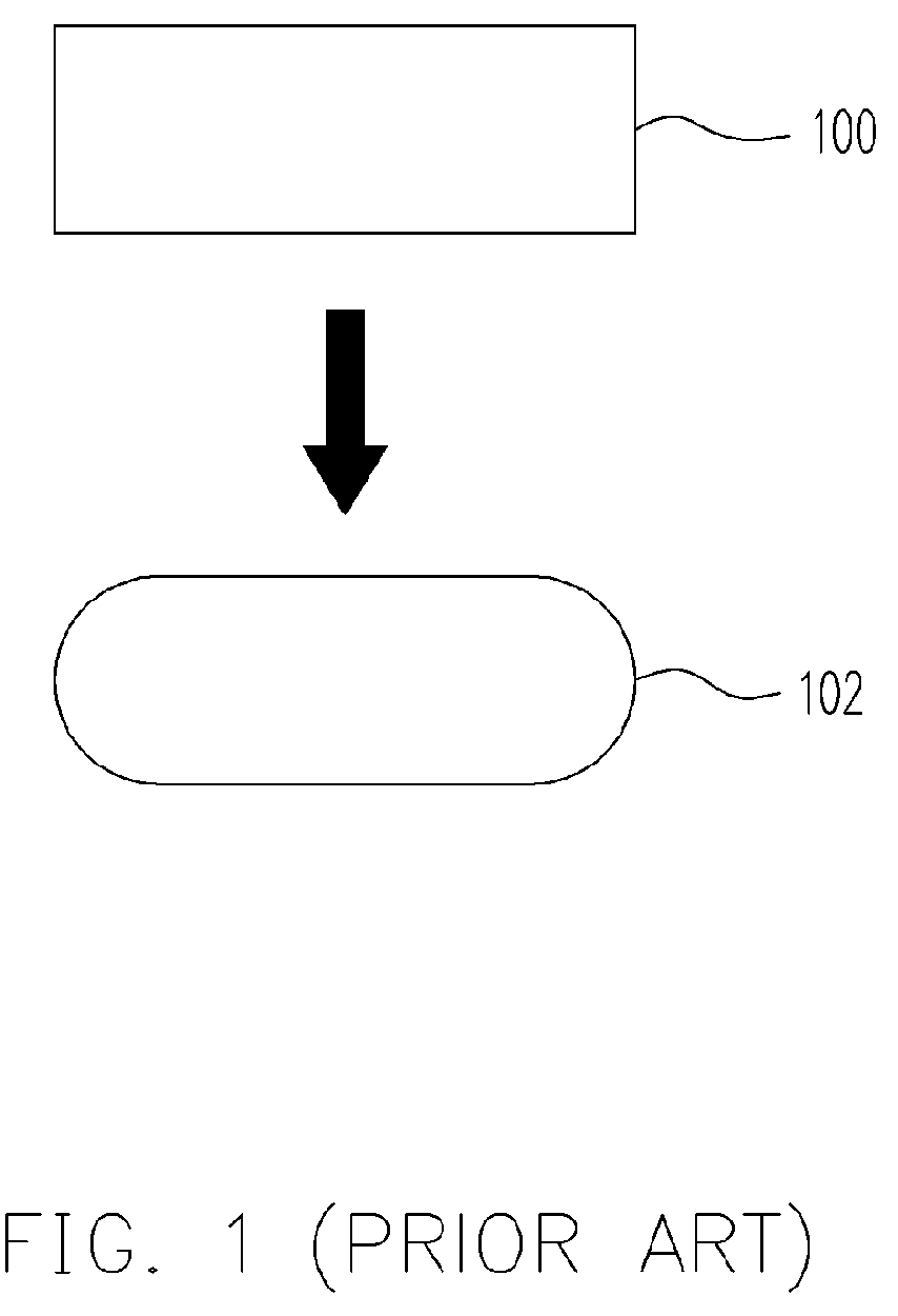
[0027]Due to dimensional deviation problem, and particularly, corner rounding problem, most mask patterning methods have undesirable consequences in subsequent fabricating processes such as a drop in the reliability and throughput and an increase in the production cost. Therefore, in the following embodiment, a mask pattern correcting apparatus and a correcting method thereof is provided.

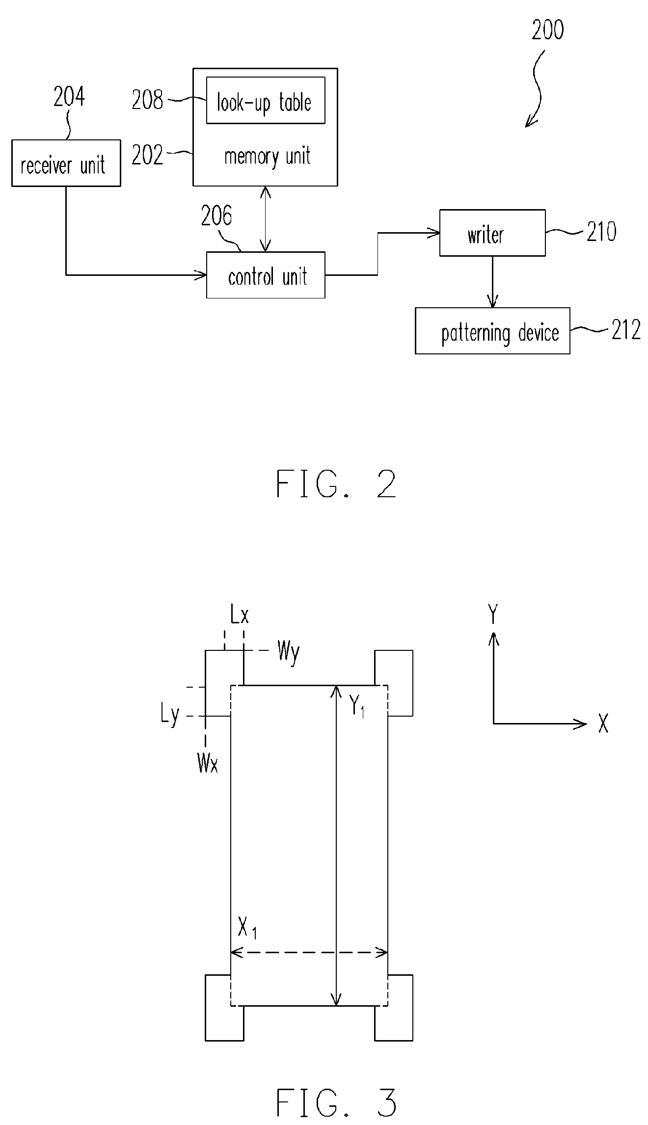
[0028]FIG. 2 is a block diagram showing a mask pattern correcting apparatus according to one embodiment of the present invention.

[0029]As shown in FIG. 2, the mask pattern correcting apparatus 200 of the present invention comprises a memory unit 202, a receiver unit 204 and a control unit 206. The memory unit 202 has...


PUM


Abstract

A method of correcting a mask pattern is provided. First, an original writer drawing data of a circuit layout pattern is inputted. Then, according to the original writer drawing data, a correcting writer rule is selected by searching from a look-up table. According to the correcting writer rule, the original writer drawing data is corrected to obtain a corrected writer drawing data of the circuit layout pattern.

Description

BACKGROUND OF THE INVENTION[0001]1. Field of the Invention[0002]The present invention relates to a photolithographic apparatus and operating method thereof, and more particularly, to a method of correcting mask pattern and correcting apparatus thereof.[0003]2. Description of the Related Art[0004]In recent years, the trend in the development of semiconductor is miniaturization of circuit devices. Among the processes used in semiconductor production, photolithographic process plays a very important role. Critical dimensions (CD) concerning semiconductor device structures, such as patterning various thin films, are dependent on the photolithographic process, which also determine the development of photolithographic technology. Thus, the accuracy of a photomask pattern is very crucial. If the pattern on the photomask is inaccurate, an inaccurate pattern will be transferred. Hence, the tolerance of the critical dimension on the chip can be affected and the resolution of the exposure can ...

Claims


Application Information

Patent Timeline
Patent Type & Authority Patents(United States)
IPC IPC(8): G06F17/50
CPCB82Y10/00B82Y40/00G03F1/144G03F1/36H01J37/3174G03F1/68
Inventor WANG, LI-MING
Owner WINBOND ELECTRONICS CORP
Why Eureka
Try Eureka