Method for material growth of GaN-based nitride layer

a gan-based nitride and material growth technology, applied in the direction of crystal growth process, polycrystalline material growth, chemically reactive gas growth, etc., can solve the problems of matter-of-fact impossible, difficult to grow a high-quality gan-based nitride layer, etc., to achieve high efficiency, excellent properties, and high reliability

Inactive Publication Date: 2008-07-01
EPIVALLEY
View PDF13 Cites 12 Cited by
  • Summary
  • Abstract
  • Description
  • Claims
  • Application Information

AI Technical Summary

Benefits of technology

[0013]According to the present invention, it is possible to grow a GaN film with excellent properties by forming a SiCN thin film, unlike the conventional film of Al(x)Ga(y)In(z)N (0≦x≦1, 0≦y≦1, 0≦z≦1, x+y+z=1), as a buffer layer on a sapphire substrate by MOCVD and forming a wetting layer and the GaN film thereon, thereby resulting in an opto-electronic device with highly efficiency and high reliability.
[0014]Also, by using a buffer layer according to the present invention, it is possible to realize LED (Light Emitting Diode) and LD (Laser Diode) with lattice mismatch between the sapphire substrate and the GaN-based nitride layer being reduced.

Problems solved by technology

However, these substrates are different from the GaN-based nitride layer in material properties such as lattice constant and thermal expansion coefficient and thus, it is difficult to grow a high quality GaN-based nitride layer.
However, it is matter-of-fact impossible.

Method used


Image

  • Method for material growth of GaN-based nitride layer
  • Method for material growth of GaN-based nitride layer
  • Method for material growth of GaN-based nitride layer

Examples


example 1

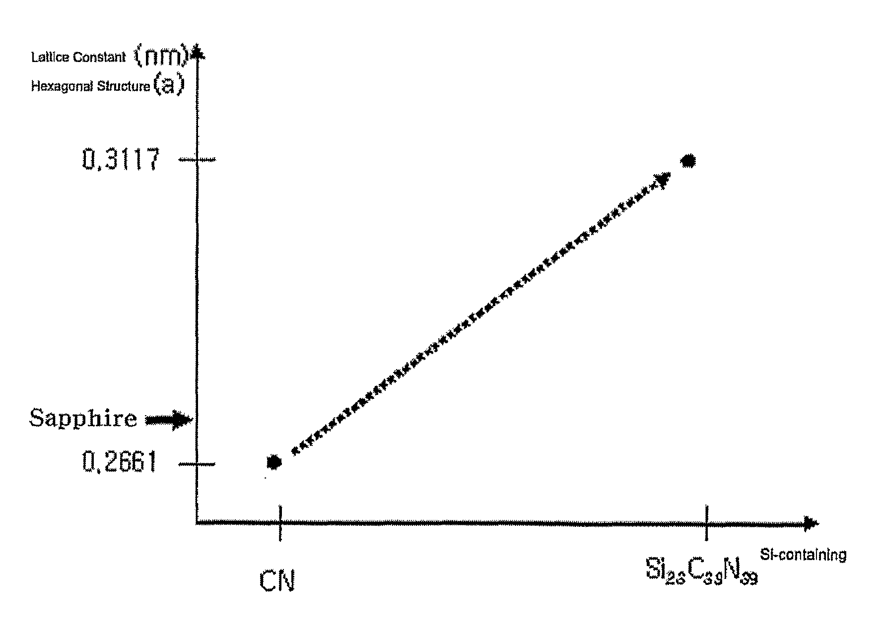
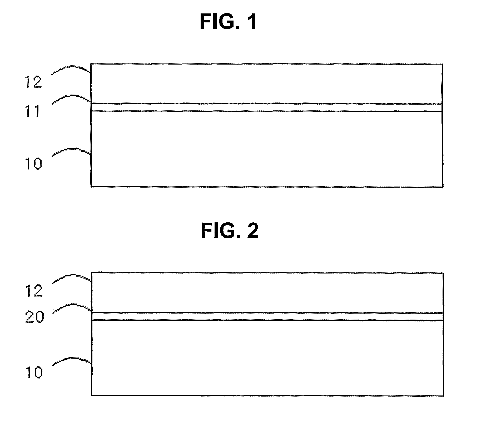
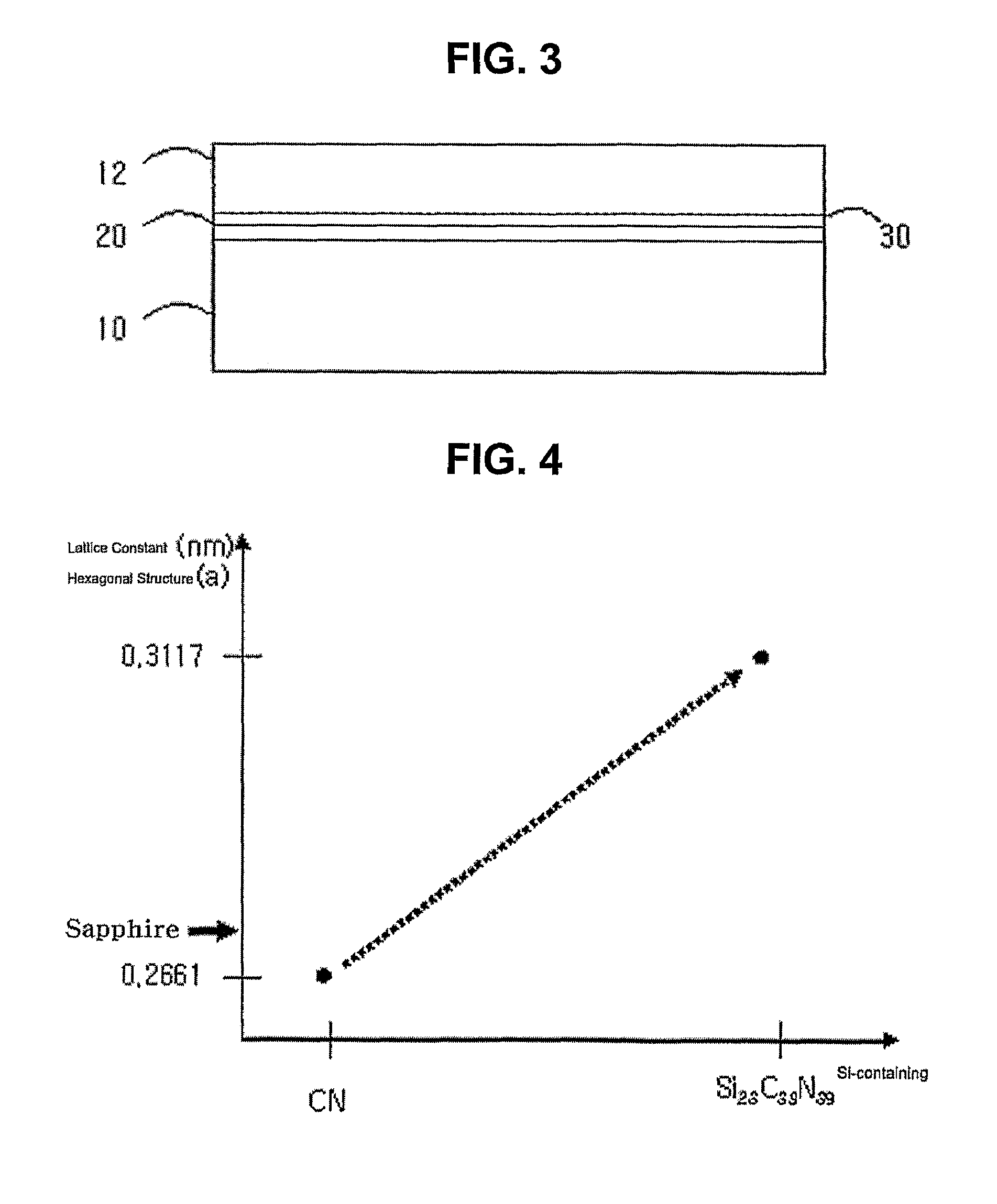
[0046]As shown in FIG. 2, a sapphire substrate 10 was initially pre-baked at a high temperature (1000° C. or higher) and a silicon carbon nitride buffer layer 20 was grown at a temperature between 900° C. and 1000° C. Here, as source materials, DTBSi, CBr4 and NH3 were used and the silicon carbon nitride buffer layer 20 was grown to a thickness of 100 Å. Hydrogen was used as a carrier gas. After completion of the formation of the silicon carbon nitride buffer layer 20, the reactor temperature was raised to 1050° C. and left to stand for stabilization of moisture. Then, a GaN film 12 was grown using TMGa and NH3.

example 2

[0047]As shown in FIG. 3, a sapphire substrate 10 was initially pre-baked at a high temperature (1000° C. or higher) and a silicon carbon nitride buffer layer 20 was grown at a temperature between 900° C. and 1000° C. Here, as source materials, DTBSi, CBr4 and NH3 were used and the silicon carbon nitride buffer layer 20 was grown to a thickness of 100 Å. Hydrogen was used as a carrier gas. Then, a wetting layer 30 comprising In0.02Ga0.98N was formed on the silicon carbon nitride buffer layer 20. Here, TMIn, TMGa and NH3 were used as source materials and the growing temperature was 800° C. Also, in the step for forming the wetting layer 30, the V to III atomic ratio (V / III ratio) was set in the range of 5000 to 6000. Then, on the wetting layer 20, a GaN film 12 was formed. Here, the GaN film 12 was grown under the conditions conventionally known to the art and generally was grown at a temperature of about 1050° C.

[0048]While the method for growing the GaN-based nitride layer has been...


PUM

PropertyMeasurementUnit
temperatureaaaaaaaaaa

Abstract

The present invention relates to a method for forming a GaN-based nitride layer comprising a first step of forming a first layer comprising SiaCbNc (c,fc>0, a≧0) on a sapphire substrate and a second step for forming a nitride layer comprising a GaN component on the first layer comprising SiaCbNc (c,b>0, a≧O).

Description

TECHNICAL FIELD[0001]The present invention relates to a method for forming a nitride layer based on gallium nitride (GaN) (herein after referred to as “GaN-based nitride layer”), and more particularly, a method for forming a GaN-based nitride layer with high quality using a silicon carbon nitride buffer layer and a wetting layer, which can be suitably used in LED (Light Emitting Diode) and LD (Laser Diode).BACKGROUND ART[0002]In preparation of semiconductor devices, a substrate comprising sapphire (Al2O3) or silicon carbide (SiC) is generally used to grow a GaN-based nitride layer. However, these substrates are different from the GaN-based nitride layer in material properties such as lattice constant and thermal expansion coefficient and thus, it is difficult to grow a high quality GaN-based nitride layer. There have been developed and disclosed many techniques for growing the GaN-based nitride layer.[0003]One of the representative methods is using a buffer layer. According to this ...

Claims


Application Information

Patent Timeline
Patent Type & Authority Patents(United States)
IPC IPC(8): H01L21/00C30B25/02C30B29/40H01L21/20H01L21/205H01L33/12H01L33/32
CPCC30B25/02C30B29/403C30B29/406H01L21/02378H01L21/02447H01L21/02488H01L21/0254H01L21/0242H01L21/0262
Inventor YOO, TAE KYUNGPARK, EUN HYUN
Owner EPIVALLEY
Why Eureka
Try Eureka