High speed, high current gain voltage buffer and method
a voltage buffer and high current gain technology, applied in amplifiers, amplifiers with semiconductor devices/discharge tubes, amplifiers, etc., can solve the problems of low current gain, frequency compensation techniques, and inability to control currents, and achieve high current gain and slew rate. high
- Summary
- Abstract
- Description
- Claims
- Application Information
AI Technical Summary
Benefits of technology
Problems solved by technology
Method used
Image
Examples
Embodiment Construction
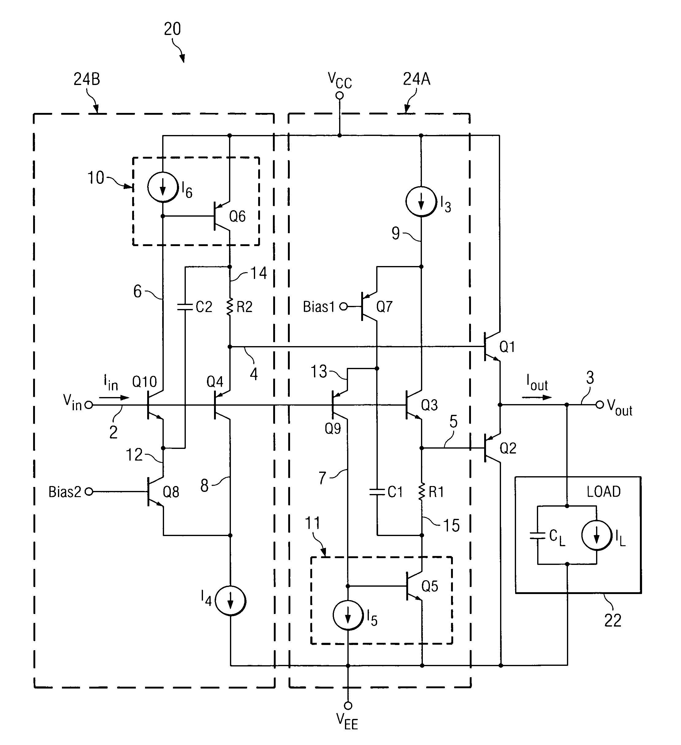
[0028]Referring to FIG. 4, in diamond buffer amplifier 20 the input voltage Vin is coupled to the bases of PNP input transistor Q4 and NPN input transistor Q3. The emitter of input transistor Q3 is coupled by conductor 5 to the base of PNP output transistor Q2 and also is coupled by isolation resistor R1 and conductor 15 to controlled current source 11. Similarly, the emitter of input transistor Q4 is coupled by conductor 4 to the base of NPN output transistor Q1 and also is coupled to one terminal of isolation resistor R2, the other terminal of which is connected by conductor 14 to an output terminal of controlled current source 10. (Isolation resistors R1 and R2 may have, for example, a resistance of roughly 1 kilohm.) Controlled current source circuit 10 includes PNP transistor Q6 and constant current source I6 connected between VCC and conductor 6, which is the control input of controlled current source 10. The emitter of PNP transistor Q6 is connected to VCC, its collector is c...
PUM
 Abstract
Description
Claims
Application Information


