ESD protection structure using contact-via chains as ballast resistors

a protection structure and contact-via chain technology, applied in the field of semiconductor dies, can solve the problems of esd failure, filamentation or thermal runaway, and it is difficult for all parts of a multi-finger fet to conduct esd current uniformly, and achieve the effect of increasing layout area, increasing esd current distribution uniformity, and not degrading high frequency performan

Active Publication Date: 2008-07-08
SKYWORKS SOLUTIONS INC
View PDF3 Cites 13 Cited by
  • Summary
  • Abstract
  • Description
  • Claims
  • Application Information

AI Technical Summary

Benefits of technology

[0009]The present invention is directed to an ESD protection structure using contact-via chains as ballast resistors. The present invention addresses and resolves the need in the art for an ESD protection structure that provides increased ESD current distribution uniformity without undesirably increasing layout area, and without degrading high frequency performance.
[0010]According to an exemplary embodiment, an ESD protection structure situated in a semiconductor die includes a FET including a gate, a first active region, and a second active region, where the gate includes at least one gate finger, and where the at least one gate finger is situated between the first active region and the second active region. The first active region can be a drain active region or a source active region, for example. The ESD protection structure further includes at least one contact-via chain connected to the first active region, where the at least one contact-via chain includes a contact connected to a via. The at least one contact-via chain forms a ballast resistor for increased ESD current distribution uniformity. The via can be situated over and in approximate alignment with the contact, for example. The at least one contact-via chain may have a resistance of approximately 10.0 ohms, for example.

Problems solved by technology

However, due to process variations and a continual scaling down of device size in advanced technologies, it is difficult for all portions of a multi-finger FET to conduct ESD current uniformly.
By localizing more ESD current, the hot-spot can cause early ESD failure in the form of filamentation or thermal runaway.
However, this approach requires a large layout area and introduces a high drain-to-bulk parasitic capacitance, which severely degrades device high frequency performance.
However, the N well resistor also requires a large layout area and undesirably introduces high parasitic N well-to-bulk capacitance to the drain, thereby severely degrading device high frequency performance.
However, in this approach, an increase in ballast resistance requires a corresponding increase in the length of each segmented active strip, which undesirable increases layout area.
By increasing the layout area, drain-to-bulk and / or source-to-bulk parasitic capacitance is also increased, which degrades high frequency performance of the device.

Method used


Image

  • ESD protection structure using contact-via chains as ballast resistors
  • ESD protection structure using contact-via chains as ballast resistors
  • ESD protection structure using contact-via chains as ballast resistors

Examples


Embodiment Construction

[0014]The present invention is directed to an ESD protection structure using contact-via chains as ballast resistors. The following description contains specific information pertaining to the implementation of the present invention. One skilled in the art will recognize that the present invention may be implemented in a manner different from that specifically discussed in the present application. Moreover, some of the specific details of the invention are not discussed in order not to obscure the invention.

[0015]The drawings in the present application and their accompanying detailed description are directed to merely exemplary embodiments of the invention. To maintain brevity, other embodiments of the present invention are not specifically described in the present application and are not specifically illustrated by the present drawings.

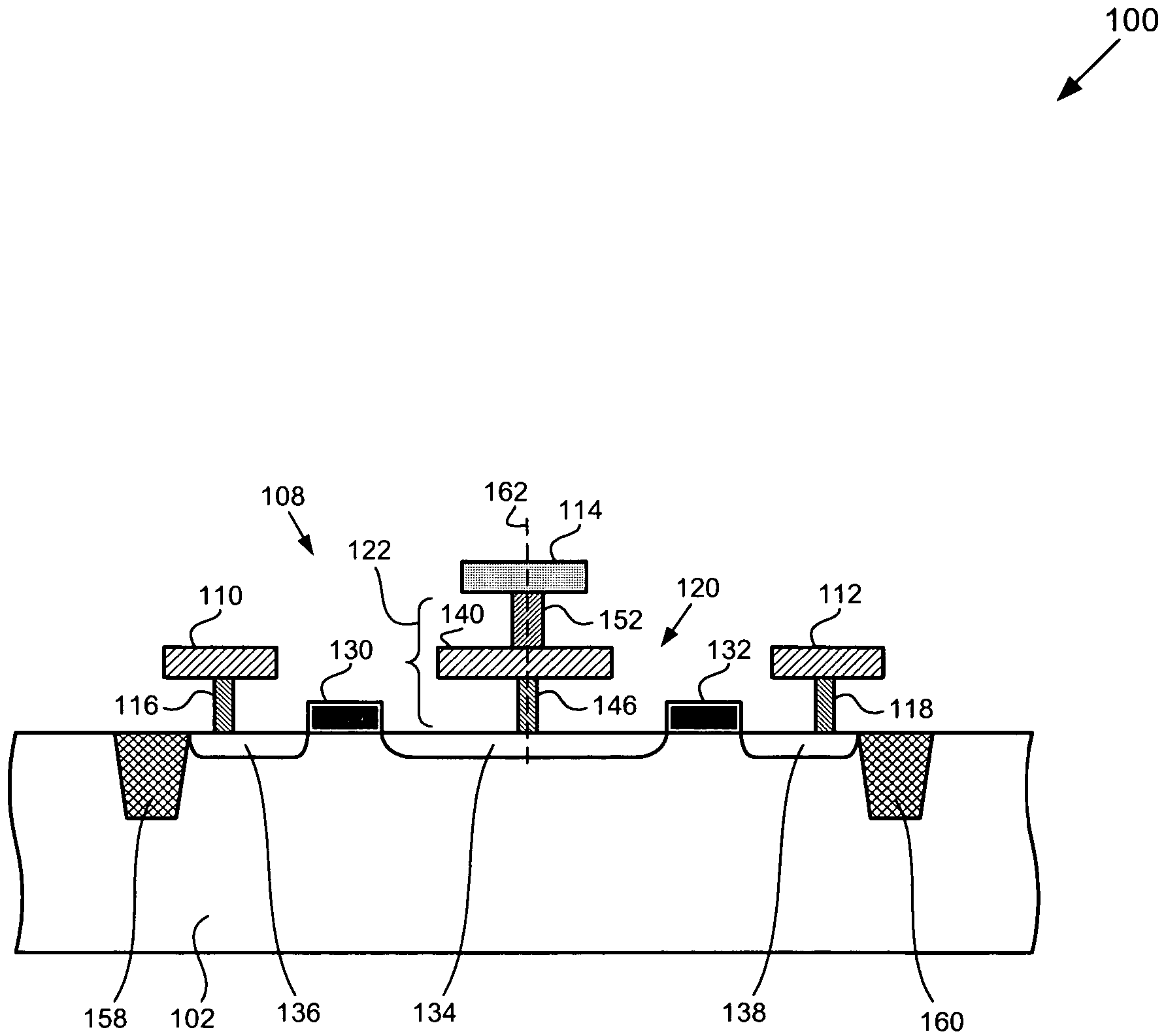
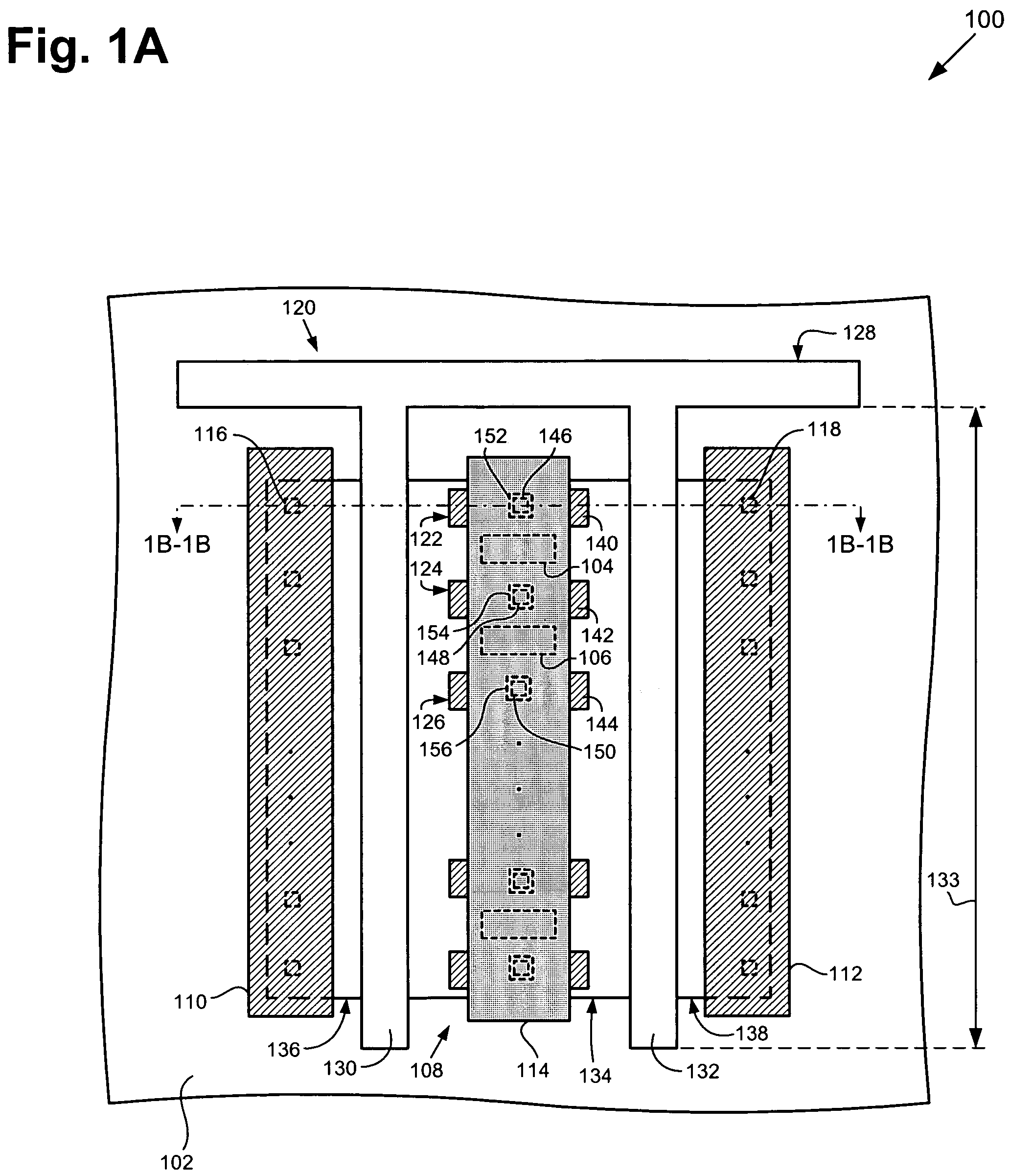
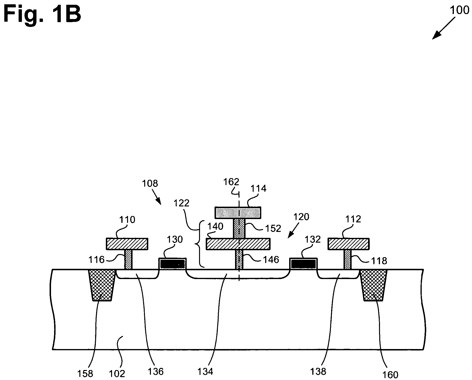
[0016]FIG. 1A shows a top view of a portion of a semiconductor die including an exemplary ESD protection structure in accordance with one embodiment ...


PUM


Abstract

According to an exemplary embodiment, an ESD protection structure situated in a semiconductor die includes a FET including a gate and first and second active regions, where the gate includes at least one gate finger, and where the at least one gate finger is situated between the first and second active regions. The ESD protection structure further includes at least one contact-via chain connected to the first active region, where the at least one contact-via chain includes a contact connected to a via. The at least one contact-via chain forms a ballast resistor for increased ESD current distribution uniformity. The contact is connected to the via by a first metal segment situated in a first interconnect metal layer of a die. The at least one contact-via chain is connected between the first active region and a second metal segment situated in a second interconnect metal layer of the die.

Description

BACKGROUND OF THE INVENTION[0001]1. Field of the Invention[0002]The present invention is generally in the field of semiconductors. More particularly, the invention is in the field of ESD protection structures in semiconductor dies.[0003]2. Background Art[0004]“Multi-finger” FETs, such as multi-finger MOSFETs, are used as a major electrostatic discharge (ESD) component in many CMOS applications. In order to discharge ESD current uniformly, a multi-finger FET should be designed such that all portions of the multi-finger FET turn on simultaneously. However, due to process variations and a continual scaling down of device size in advanced technologies, it is difficult for all portions of a multi-finger FET to conduct ESD current uniformly. Thus, a portion of the multi-finger FET may turn on faster than another portion of the multi-finger FET and become “a hot-spot,” which can localize more ESD current. By localizing more ESD current, the hot-spot can cause early ESD failure in the form ...

Claims


Application Information

Patent Timeline
Patent Type & Authority Patents(United States)
IPC IPC(8): H01L23/62
CPCH01L27/0266H01L29/41725H01L29/41758H01L29/78H01L27/0629H01L29/0692H01L2924/0002H01L2924/00H01L23/62H01L23/60
Inventor ZHANG, JIONGCHENG, YUHUA
Owner SKYWORKS SOLUTIONS INC
Why Eureka
Try Eureka