Voltage level translator circuit with wide supply voltage range

a voltage level translator and supply voltage technology, applied in logic circuit coupling/interface arrangement, pulse technique, instruments, etc., can solve the problems of slow speed, inoperable standard voltage level translator circuits, slow speed, etc., and achieve the effect of constant propagation delay

Active Publication Date: 2008-07-08
AVAGO TECH INT SALES PTE LTD
View PDF12 Cites 21 Cited by
  • Summary
  • Abstract
  • Description
  • Claims
  • Application Information

AI Technical Summary

Benefits of technology

[0005]The present invention meets the above-noted need by providing, in an illustrative embodiment, a voltage translator circuit capable of interfacing between multiple voltage levels, such as, for example, between an input signal, which is referenced to a lower core voltage supply of the circuit, and an output signal, which is referenced to a higher voltage supply of the circuit. Based at least in part on a difference between the higher voltage supply and the lower core voltage supply, the voltage translator circuit is advantageously configured to select one of at least two different reference voltage levels to thereby enable the voltage level translator circuit to operate over a wider supply voltage range compared to standard voltage level translator circuits. Moreover, the voltage level translator circuit of the present invention employs one signal path, and thus the circuit exhibits a substantially constant propagation delay regardless of the level of the higher voltage supply.

Problems solved by technology

However, this approach significantly increases the cost of both design and fabrication of the circuits, and is thus undesirable.
It is well known that when the IO voltage source is brought down to a level comparable to the core voltage source level, such as, for instance, to conserve power, a standard voltage level translator circuit is often inoperable or operates with poor performance (e.g., slower speed, increased skew, etc.).
Thus, standard voltage level translator circuits that are designed to handle a wide range of IO voltage source levels typically do so by compromising on circuit performance.

Method used


Image

  • Voltage level translator circuit with wide supply voltage range
  • Voltage level translator circuit with wide supply voltage range
  • Voltage level translator circuit with wide supply voltage range

Examples


Embodiment Construction

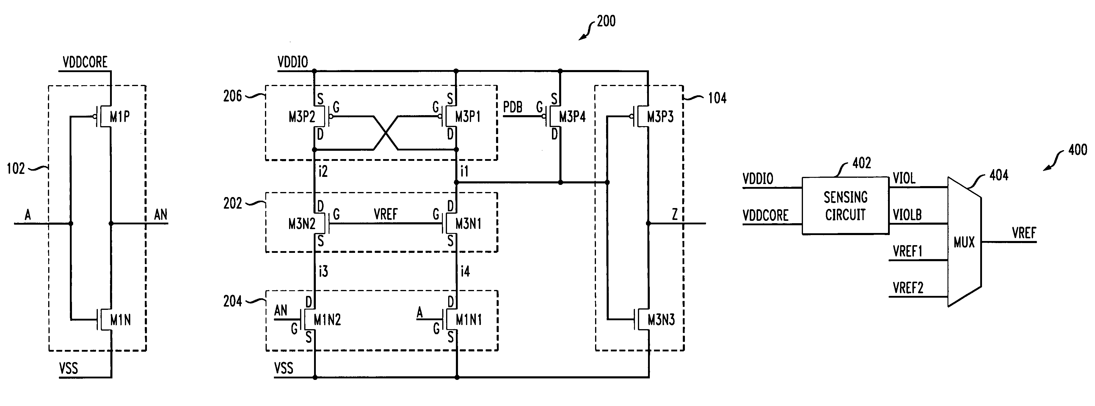
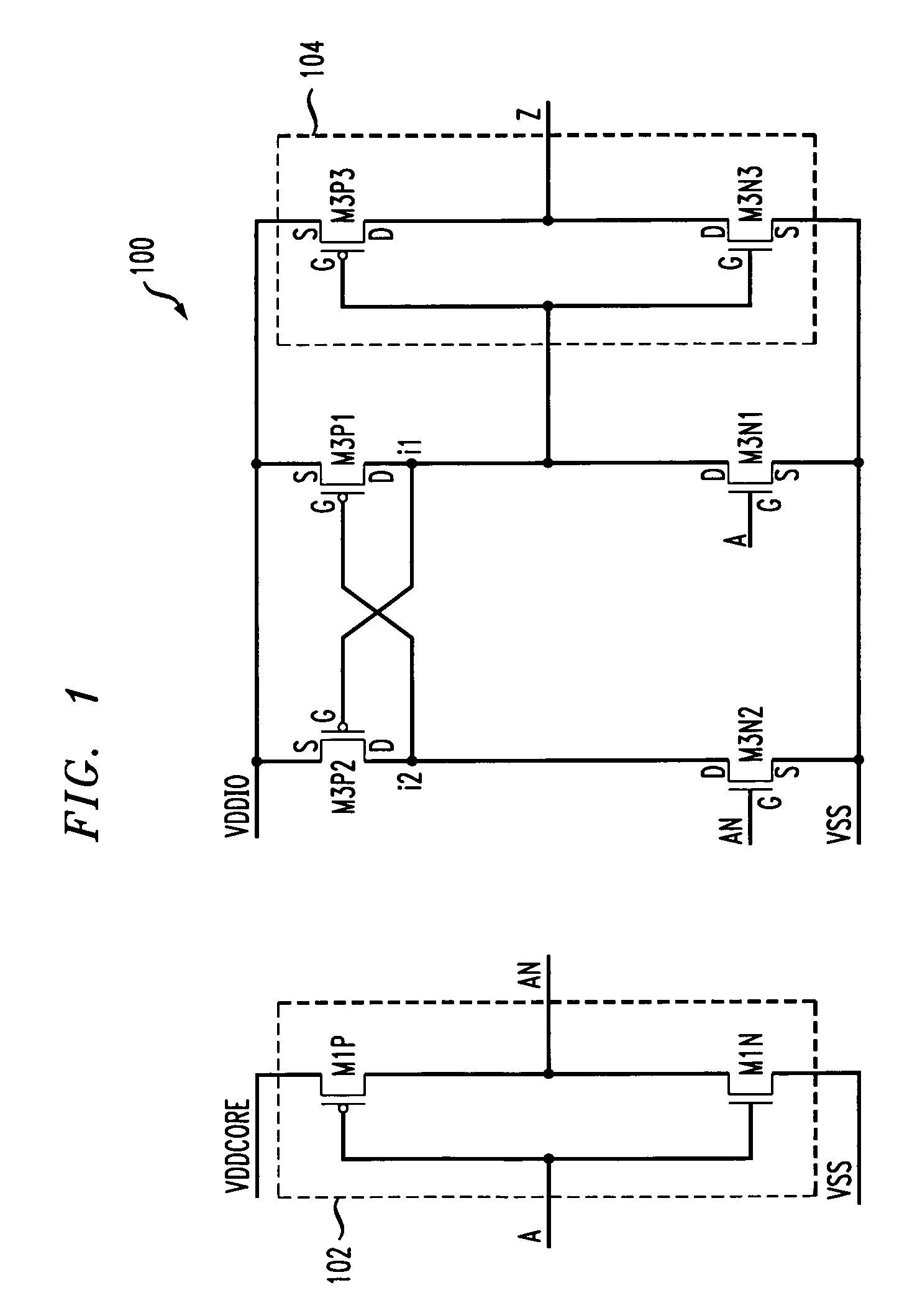
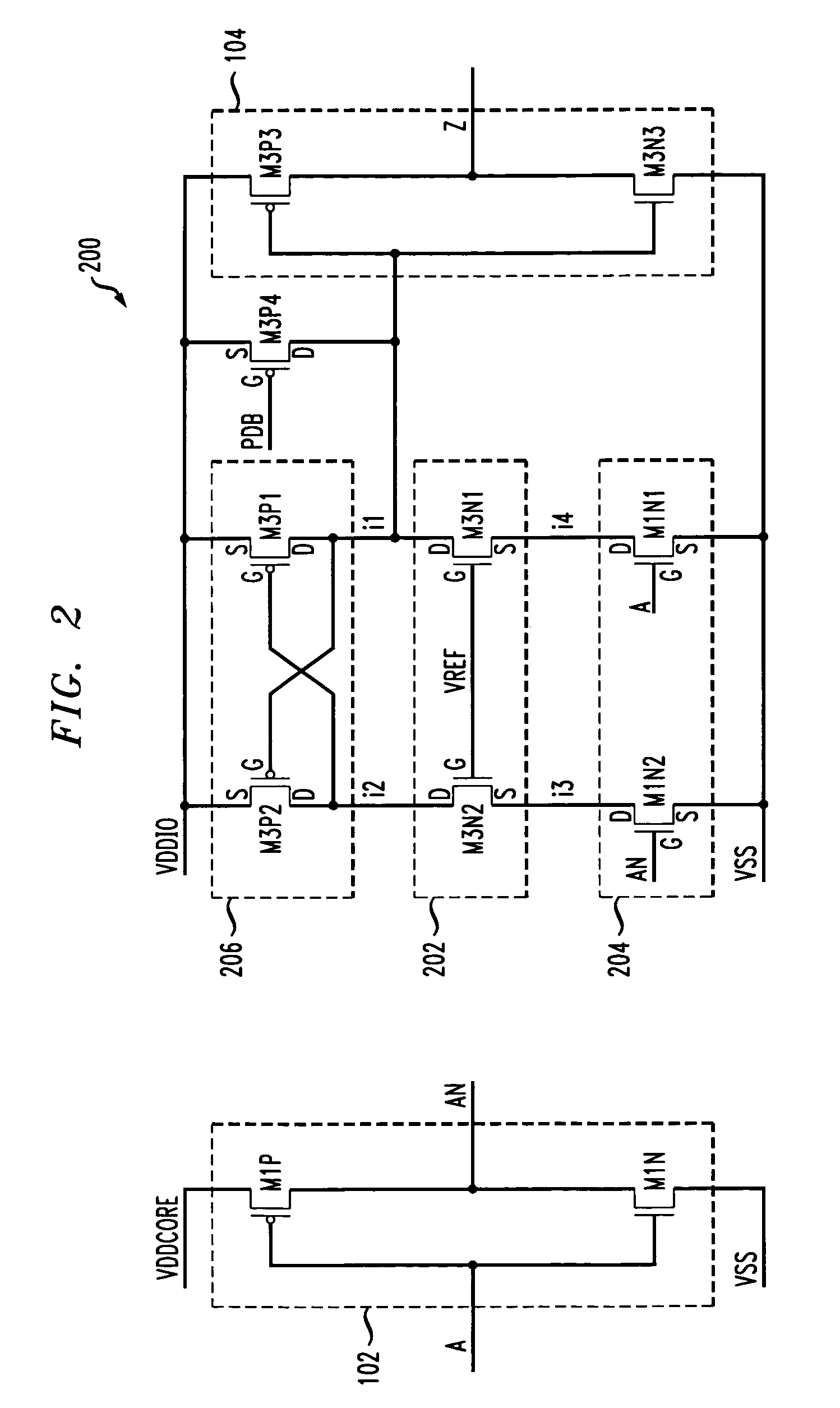
[0019]The present invention will be described herein in the context of illustrative voltage level translator circuits. It should be understood, however, that the present invention is not limited to these or any other particular circuit arrangements. Rather, the invention is more generally applicable to techniques for interfacing between multiple voltage levels in a circuit without suffering any significant degradation in circuit performance over a wide range of supply voltage levels, particularly when a higher voltage supply, to which the output signal of the circuit is referenced, is substantially close in value to a lower core supply, to which an input signal to the circuit is referenced. Although implementations of the present invention are described herein with specific reference to P-channel metal-oxide-semiconductor (PMOS) and N-channel metal-oxide-semiconductor (NMOS) transistor devices, as may be formed using a complementary metal-oxide-semiconductor (CMOS) fabrication proce...


PUM


Abstract

A voltage level translator circuit for translating an input signal referenced to a first voltage supply to an output signal referenced to a second voltage supply includes an input stage for receiving the input signal, the input stage including at least one transistor device having a first threshold voltage associated therewith. The voltage level translator circuit further includes a latch circuit operative to store a signal representative of a logic state of the input signal, the latch circuit including at least one transistor device having a second threshold voltage associated therewith, the second threshold voltage being greater than the first threshold voltage. A voltage clamp circuit is connected between the input stage and the latch circuit. The voltage clamp circuit is operative to limit a voltage across the input stage, an amplitude of the voltage across the input stage being controlled as a function of a voltage difference between the first and second voltage supplies.

Description

FIELD OF THE INVENTION[0001]The present invention relates generally to electronic circuits, and more particularly relates to voltage level translator circuits.BACKGROUND OF THE INVENTION[0002]Certain portable devices, including wireless handsets, notebook computers and personal digital assistants (PDAs), often employ circuitry which runs on two or more different voltage levels. For instance, circuitry utilized with such portable devices may be configured so that a portion of the circuitry, such as, for example, input / output (IO) buffers, runs at a higher voltage level (e.g., about 3.3 volts), as may be supplied by an IO voltage source, while another portion of the circuitry, such as, for example, core logic, runs at a substantially lower voltage level (e.g., about 1.0 volt), as may be supplied by a core voltage source. This difference in voltage levels often necessitates the use of a voltage level translator circuit for interfacing between the multiple voltage levels.[0003]There are...

Claims


Application Information

Patent Timeline
Patent Type & Authority Patents(United States)
IPC IPC(8): H03K19/0175H03K5/00
CPCH03K19/017509H03K3/356104G05F1/40G11C5/14H02M3/04
Inventor BHATTACHARYA, DIPANKARKOTHANDARAMAN, MAKESHWARKRIZ, JOHN C.MORRIS, BERNARD L.SIMKO, JOSEPH E.
Owner AVAGO TECH INT SALES PTE LTD
Why Eureka
Try Eureka