
Input tracking high-level multibit quantizer for delta-sigma ADC

a multi-level, input tracking technology, applied in the field of multi-level quantizers, can solve the problems of insufficient to overcome the above mentioned shortcomings, insufficient delay requirement, serious limit the practical options for the topology of multi-level quantizers, etc., to achieve small internal integrator output signal swing, reduce chip area, and reduce power

Active Publication Date: 2008-07-08
TEXAS INSTR INC
View PDF4 Cites 11 Cited by
  • Summary
  • Abstract
  • Description
  • Claims
  • Application Information

AI Technical Summary

Benefits of technology

The proposed solution significantly reduces power consumption and die area while providing small internal integrator output signal swings and improved modulator stability, making it suitable for high-performance, low-power delta-sigma ADCs.

Problems solved by technology

It also requires additional digital to analog converter (DAC) circuits, and suffers from potential modulator instability due to parasitic high frequency input signal leakages and the like.
The foregoing reference discloses the common technique of using a simplified first order dynamic element matching (DEM) circuit, but that is insufficient to overcome the above mentioned shortcomings.
This minimum delay requirement seriously limits the practical options for the topology of the multilevel quantizer.
Flash type ADCs are normally used as quantizers due to their low latency, which refers to time delay between the outputs and inputs thereof.
However, it is well-known that flash ADCs are characterized by low efficiency and low resolution.
Compared with other ADCs, such as SAR or pipeline ADCs, a flash ADC consumes more power and requires more die area, even though the latency of a flash ADC is lower than the other types.
Although increasing quantizer resolution / quantizer levels inside multilevel delta-sigma ADCs reduces output swings (and hence also the power consumption) of the integrators, reduces quantization noise, and decreases performance sensitivity to clock jitter, the low efficiency of conventional flash-based quantizer designs results in excessive power consumption and excessive die area and therefore diminishes the advantages of increased quantizer resolution / quantizer levels of the conventional flash-based quantizers.
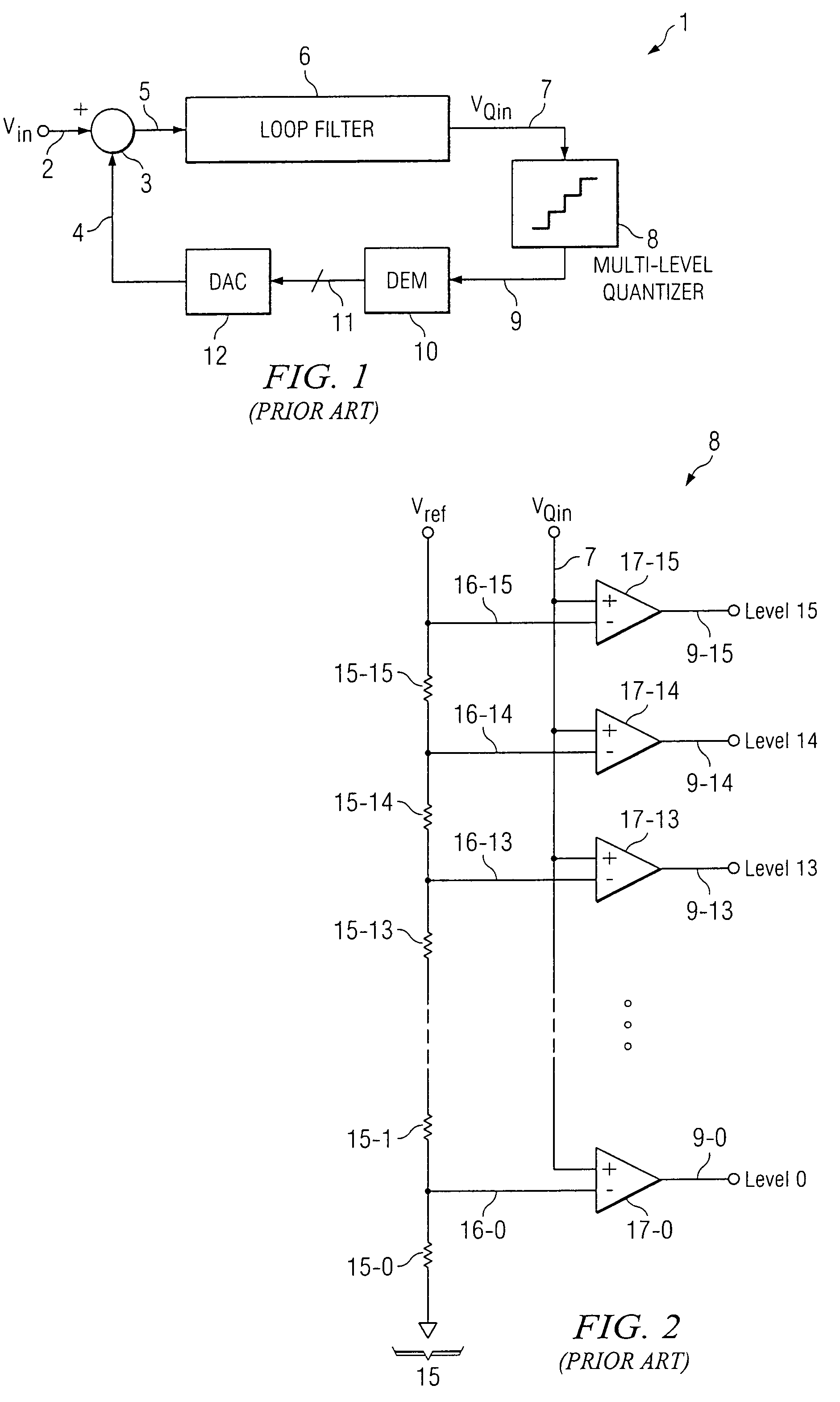
Conventional flash type quantizers of the type shown in FIG. 2 are considered to be very inefficient and not suitable for many future converter designs.
There also is an unmet need for an improved quantizer topology which requires simpler control logic circuitry, consumes much lower power, and requires less die area than the prior art flash-based quantizer designs.

Method used


Image

  • Input tracking high-level multibit quantizer for delta-sigma ADC
  • Input tracking high-level multibit quantizer for delta-sigma ADC
  • Input tracking high-level multibit quantizer for delta-sigma ADC

Examples


Embodiment Construction

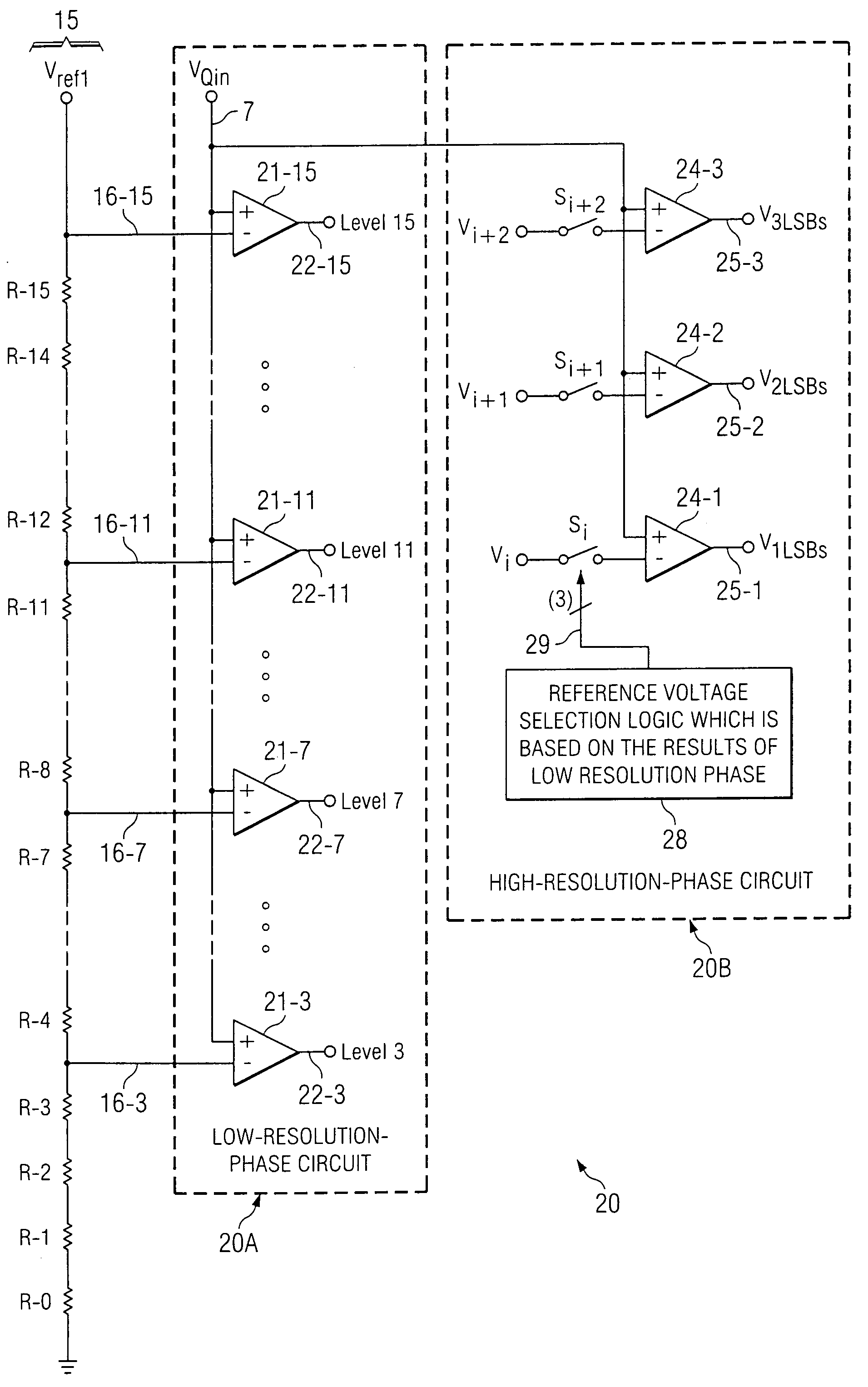
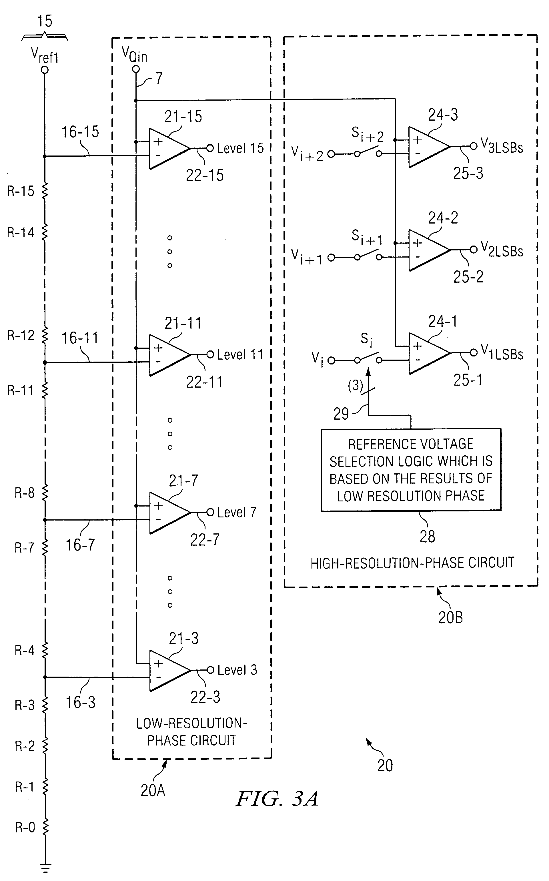
[0029]A generalized diagram of a 16-level quantizer according to the present invention and its timing diagram are shown in FIGS. 3A and 4, respectively. Referring to FIG. 3A, two-phase multilevel quantizer 20 includes a resistor string 15A, a low-resolution-phase circuit 20A, and a high-resolution-phase circuit 20B. Resistor string 15A includes, for example, 16 precision resistors R-0,1,2 . . . 15 coupled between a reference voltage Vref1 and ground. Four of the tap points, labeled 16-3, 16-7, 16-11, and 16-15 are coupled to the (−) inputs of four comparators 21-3, 21-7, 21-11, and 21-15, respectively, of low-resolution-phase circuit 20A. Tap point 16-3 is connected to the junction between resistors R-3 and R-4. Similarly, tap point 16-7 is connected to the junction between string resistors R-7 and R-8, tap point 16-11 is connected to the junction between string resistors R-11 and R-12, and tap point 16-15 is connected to Vref1.

[0030]The (+) inputs of comparators 21-3, 21-7, 21 -11,...


PUM


Abstract

A quantization circuit includes a plurality of resistors, a plurality of tap points, and a plurality of coarse comparators. Each coarse comparator has a first input coupled to an input voltage and a second input coupled to a corresponding coarse tap point voltage. Each coarse comparator operates during a first phase to produce a “1” only if the input voltage exceeds the corresponding coarse tap point voltage. A plurality of fine comparators each have a first input coupled to the input voltage, and each fine comparator operates during a second phase to produce a fine output level indicative of whether the input voltage exceeds a corresponding tap point voltage of a group of tap points located immediately below the tap point connected to the highest coarse comparator producing a “1”.

Description

CROSS REFERENCE TO RELATED APPLICATION[0001]This application claims the benefit of prior filed now abandoned U.S. provisional application Ser. No. 60 / 824,232 filed Aug. 31, 2006, entitled “Efficient Digital Controlled Multilevel Quantizer Design for High Performance Sigma-Delta ADC”, by YuQing Yang, and incorporated herein by reference.BACKGROUND OF THE INVENTION[0002]The present invention relates generally to multilevel quantizers, particularly two-phase multilevel quantizers designed to be implemented in reduced amounts of chip area and also designed to dissipate reduced amounts of power. The invention also relates more particularly to high-performance, low-power delta-sigma modulators and delta sigma analog-to-digital converters (ADCs) which include such two-stage multilevel quantizers.[0003]The closest prior art is believed to be represented by the article “A 3-mW 74-dB SNR 2-MHz Continuous-Time Delta-Sigma ADC With a Tracking ADC Quantizer in 0.13-μm CMOS” by Lukas Dörrer et al...

Claims


Application Information

Patent Timeline
Patent Type & Authority Patents(United States)
IPC IPC(8): H03M1/12
CPCH03M1/146H03M3/424H03M1/361H03M3/452H03M1/365
Inventor YANG, YUQING
Owner TEXAS INSTR INC
Learn More