

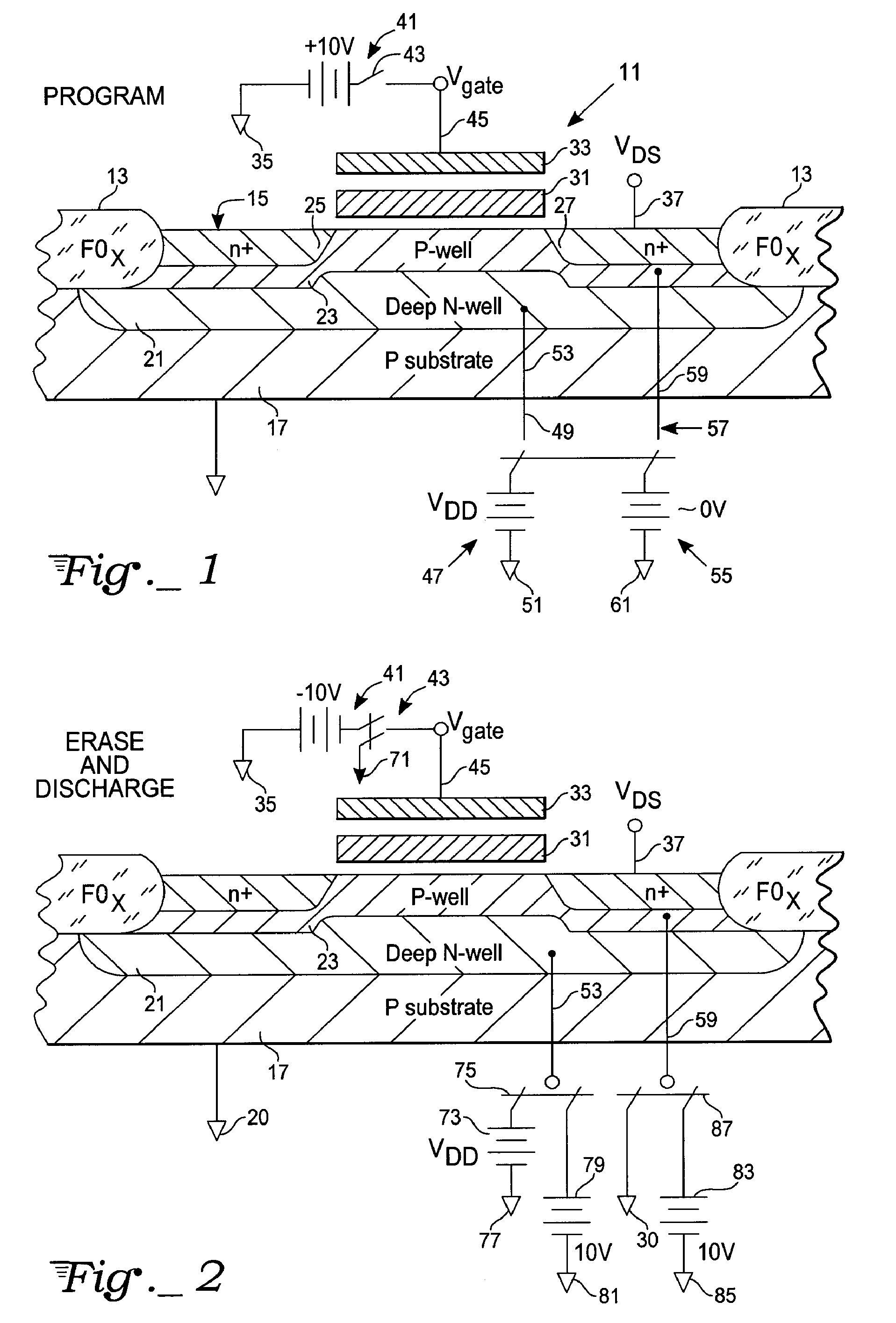
Channel discharging after erasing flash memory devices
a flash memory device and channel discharge technology, applied in semiconductor devices, digital storage, instruments, etc., can solve problems such as device latchup, and achieve the effect of relaxing any demand on high voltage supply and shortening supply of high capacity
- Summary
- Abstract
- Description
- Claims
- Application Information
AI Technical Summary
Benefits of technology
Problems solved by technology
Method used
Image

Examples
Embodiment Construction
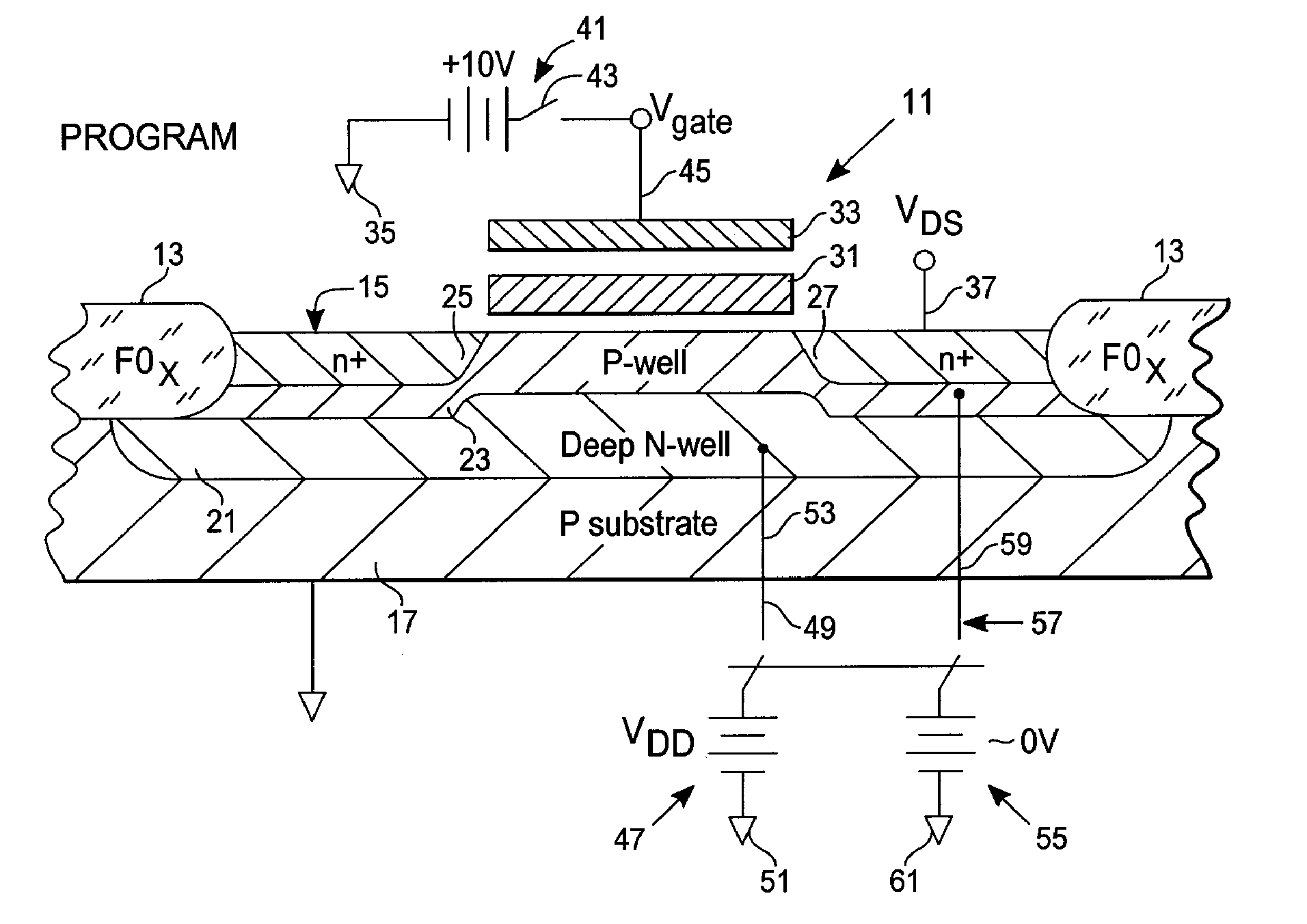
[0012]With reference to FIG. 1, a non-volatile memory cell 11, typically an EEPROM (electrically erasable programmable read only memory) transistor, is constructed within a silicon wafer or substrate 17, shown as a p-type substrate. Within this substrate the memory cell 11, an EEPROM device, is built within an active region defined by a field oxide FOX boundary 13. The substrate has a surface 15, with portions of the device above the surface and portions below.
[0013]Below surface 15, a deep N-well 21 is established in substrate 17, overlapping with the field oxide boundaries FOX 13 across the entire subsurface regions of the device, by implantation or diffusion of n-type ionic impurities in a known manner. After N-well 21 is established a less deep P-well 23 is established within the upper half, more or less, of the deep N-well 21. The P-well 23 extends from surface 15 downwardly to about one-half of the depth of the N-well 21 and from one field oxide boundary to the other. Building...
PUM
 Abstract
Description
Claims
Application Information