Refractory metal capped low resistivity metal conductor lines and vias formed using PVD and CVD

a technology of refractory metal and capped metal, which is applied in the direction of electrical apparatus, semiconductor devices, semiconductor/solid-state device details, etc., can solve the problems of failure to meet the requirements of the application

Inactive Publication Date: 2001-11-27
GLOBALFOUNDRIES INC
View PDF137 Cites 115 Cited by
  • Summary
  • Abstract
  • Description
  • Claims
  • Application Information

AI Technical Summary

Benefits of technology

It is therefore an object of the present invention to provide low-cost, corrosion-free, wear-resistant, electromigration resistant, electrical conductor interconnecting circuits on a substrate on a submicron scale using a method with a high process yield.

Problems solved by technology

Today's emphasis on scaling down line width dimensions in very large scale integrated (VLSI) circuitry manufacture has led to reliability problems including inadequate isolation, electromigration, and planarization.
However, the tungsten layer formed using the low temperatures described by Ahn et al. would be silicon rich (e.g., 3-4%) and would not be a good diffusion barrier for copper since copper resistivity would be degraded by the formation of copper silicide.
Thus, it is difficult to deposit a diffusion barrier by selective means at low temperature.
The creation of the donut shape is believed to be not reliable.
It is difficult to achieve planarity of the dielectric using RIE.
Planarity is in part dependent on the pattern density, and non-planar surfaces result in puddling problems during subsequent metalization.
RIE of any high copper content, aluminum or copper alloy is extremely difficult.
A serious drawback of traditional processes which include metal RIE is that a large number of metal shorts tend to develop with fine geometry due to particle defects.
The Brown et al. method does not avoid metal corrosion and other problems associated with etching and is not useful for planarizing Al--Cu or other soft alloys because they have different properties from the harder metals such as tungsten and molybdenum.
Moreover, using the Brown et al. method, it is difficult to completely fill vias and lines.
Neither Beyer et al. nor Cote et al. recognize that polishing is not practical for low resistivity, soft metals such as Al--Cu alloys.
This is because such materials tend to scratch, smear on the surface, and corrode under the influence of the slurry.
Moreover, creation of the planarized structures in accordance with Cote et al. takes several processing steps which increases costs and reduces output.

Method used


Image

  • Refractory metal capped low resistivity metal conductor lines and vias formed using PVD and CVD
  • Refractory metal capped low resistivity metal conductor lines and vias formed using PVD and CVD
  • Refractory metal capped low resistivity metal conductor lines and vias formed using PVD and CVD

Examples


Embodiment Construction

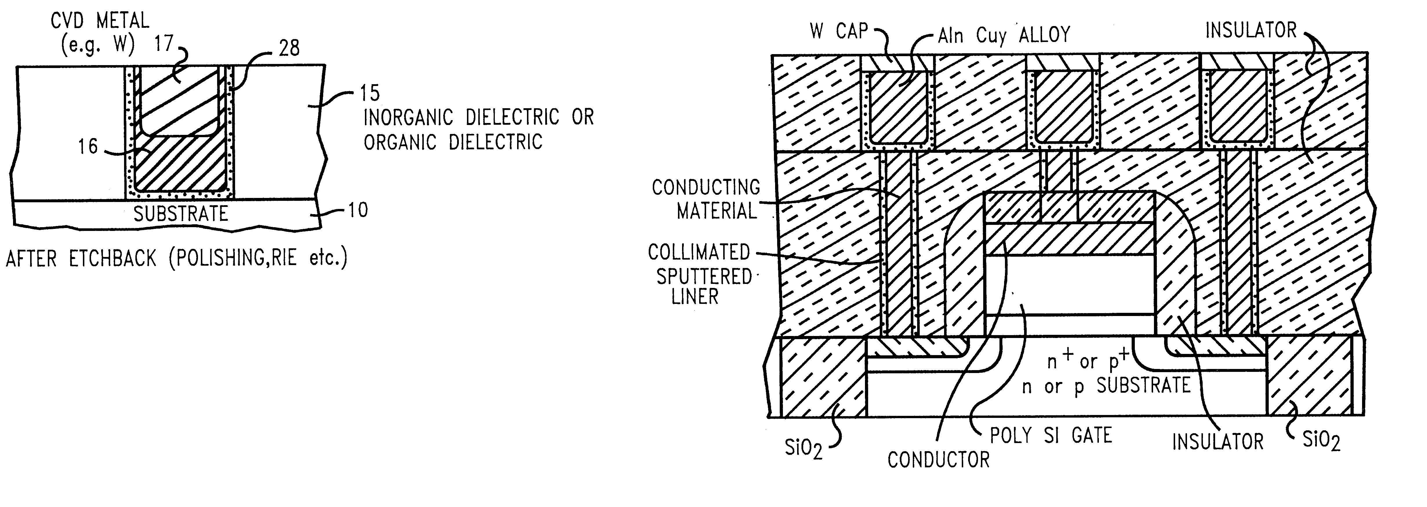
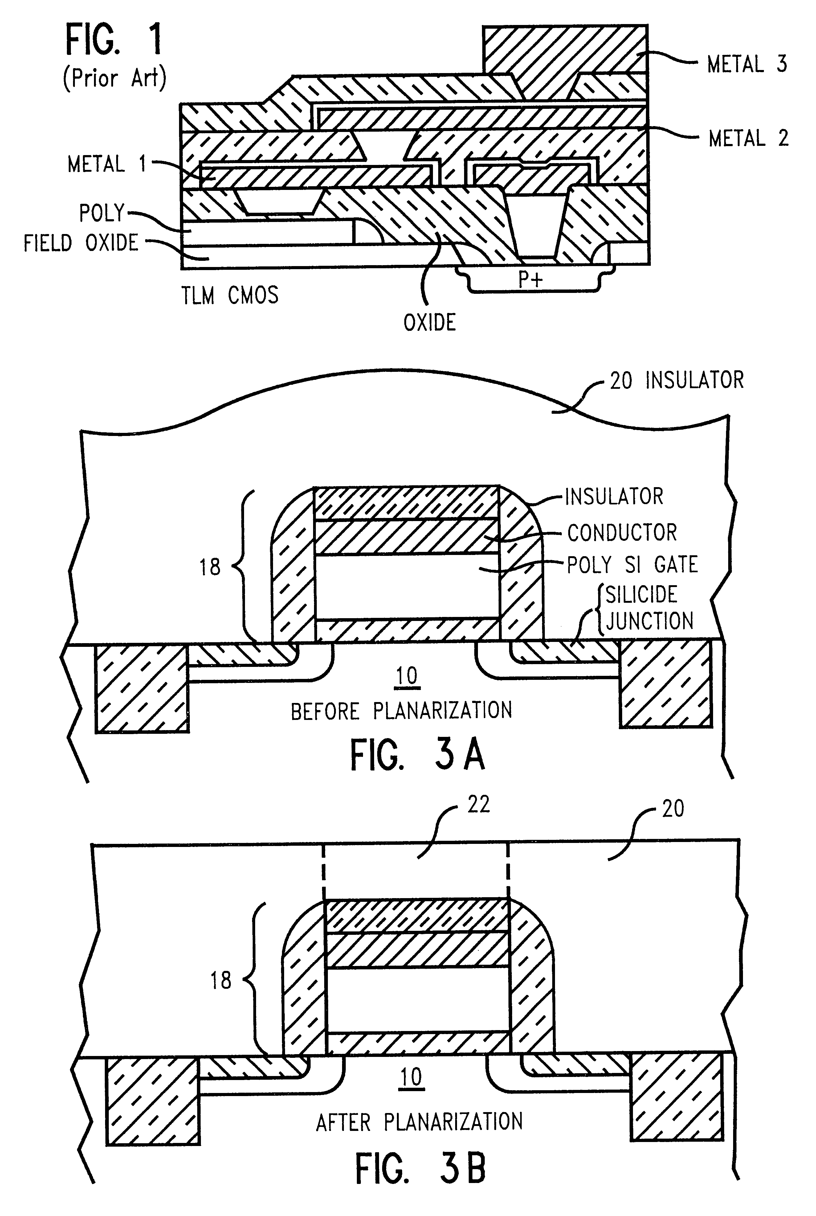
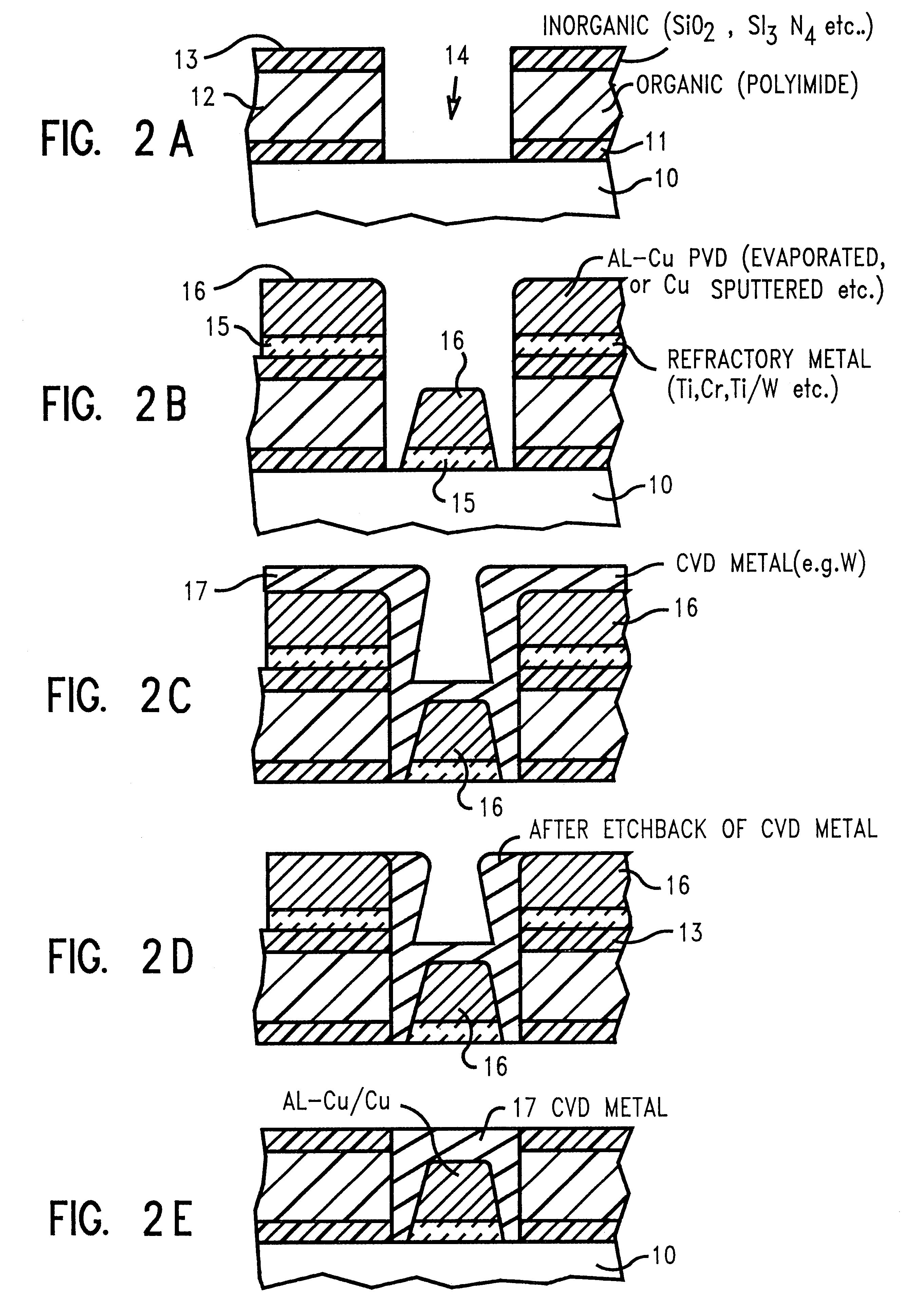
The invention is generally related to methods for forming metal filled vias and conductor lines on a substrate where the vias and conductor lines include a soft, low resistivity metal which is capped with a relatively hard, refractory metal which is resistant to corrosion, wear, and electromigration, and where the vias and conductor lines are planar with a dielectric layer coated on the substrate. Several different and novel structures are created according to the procedures described in conjunction with FIGS. 2A-E, FIGS. 4A-E, and FIGS. 7A-B, depending on the PVD deposition technique utilized. It should be understood that the techniques and resulting structures are not limited to using any specific substrates and dielectric overlays (e.g., composites of inorganic and organic layers like that shown in FIGS. 2A-E and 5A-E can be used as well as single layers of inorganic or organic insulator materials). Moreover, the invention is not restricted to any particular metal combinations; r...


PUM

PropertyMeasurementUnit
depthaaaaaaaaaa
pressuresaaaaaaaaaa
pressuresaaaaaaaaaa

Abstract

Capping a low resistivity metal conductor line or via with a refractory metal allows for effectively using chemical-mechanical polishing techniques because the hard, reduced wear, properties of the refractory metal do not scratch, corrode, or smear during chemical-mechanical polishing. Conductive lines and vias are created using a combination of both physical vapor deposition (e.g., evaporation or collimated sputtering) of a low resistivity metal or alloy followed by chemical vapor deposition (CVD) of a refractory metal and subsequent planarization. Altering a ratio of SiH4 to WF6 during application of the refractory metal cap by CVD allows for controlled incorporation of silicon into the tungsten capping layer. Collimated sputtering allows for creating a refractory metal liner in an opening in a dielectric which is suitable as a diffusion barrier to copper based metalizations as well as CVD tungsten. Ideally, for faster diffusing metals like copper, liners are created by a two step collimated sputtering process wherein a first layer is deposited under relatively low vacuum pressure where directional deposition dominates (e.g., below 1 mTorr) and a second layer is deposited under relatively high vacuum pressure where scattering deposition dominates (e.g., above 1 mTorr). For refractory metals like CVD tungsten, the liner can be created in one step using collimated sputtering at higher vacuum pressures.

Description

1. Field of the InventionThe present invention generally relates to the manufacture of electrical conductor lines and vias that interconnect circuits on substrates such as semiconductors and related packages and, more particularly, to a low cost method of filling seams or holes in substrates using a combination of a low resistivity metal deposited by physical vapor deposition (PVD) and a refractory metal deposited by chemical vapor deposition (CVD). The invention has particular application in submicron circuit manufacture.2. Description of the Prior ArtLow resistivity metals such as aluminum and copper and their binary and ternary alloys have been widely explored as fine line interconnects in semiconductor manufacturing. Typical examples of fine line interconnect metals include Al.sub.x Cu.sub.y, where the sum of x and y is equal to one and both x and y are greater than or equal to zero and less than or equal to one, ternary alloys such as Al--Pd--Cu and Al--Pd--Nb, Al--Cu--Si, and ...

Claims


Application Information

Patent Timeline
Patent Type & Authority Patents(United States)
IPC IPC(8): H01L23/532H01L21/70H01L23/52H01L21/768H01L23/498H01L23/48H01L21/02H01L21/318H01L21/316H01L21/312H01L21/28H01L23/522
CPCH01L21/76838H01L21/7684H01L21/76843H01L21/76847H01L21/76849H01L21/76852H01L21/76877H01L23/49866H01L23/53223H01L23/53228H01L23/53233H01L23/53238H01L2924/0002H01L2924/09701Y10S257/915Y10S148/015Y10S438/959H01L2924/00H01L21/76801H01L23/522
Inventor JOSHI, RAJIV V.CUOMO, JEROME J.DALAL, HORMAZDYAR M.HSU, LOUIS L.
Owner GLOBALFOUNDRIES INC
Why Eureka
Try Eureka