Singulation method and resulting device of thick gallium and nitrogen containing substrates

a nitrogen-containing substrate and sulfur-containing technology, applied in the field of lighting techniques, can solve the problems of reducing the efficiency of conventional edison light bulbs, reducing the efficiency of conventional light bulbs, and reducing the frequency of chip-outs, so as to reduce the need for expensive and time-consuming lapping and polishing steps, and reduce the incidence of chip-outs

Inactive Publication Date: 2012-11-20
KORRUS INC
View PDF30 Cites 16 Cited by
  • Summary
  • Abstract
  • Description
  • Claims
  • Application Information

AI Technical Summary

Benefits of technology

[0010]The LED wafer is laser-scribed within the ‘scribe streets’ on a first surface of the wafer, along one or more axes according to a specific embodiment. The scribe depth in the scribed regions on the first surface is typically 20-25% of the thickness of the LED wafer according to a specific embodiment. In a specific embodiment, the LED wafer is then flipped over, and is then laser-scribed within the ‘scribe streets’ on a second surface of the wafer, along one or more axes, taking care to ensure that the scribes on the second surface are aligned to be substantially overlying the scribes on the first side of the wafer. In other embodiments, scribe lines on one side may be aligned to scribe lines on the other side of the substrate In a specific embodiment, the scribe depth in the scribed regions on the second surface is typically 20-25% of the thickness of the LED wafer The scribed LED wafer is then broken using an anvil breaker setup. Breaking occurs along the planes defined by two aligned scribed regions on the two opposing sides of the wafer. In a specific embodiment, the present method allows for the singulation of thick GaN wafers, thereby eliminating the need for expensive and time-consuming lapping and polishing steps in the LED fabrication process.
[0011]The present method provides for the singulation of thick GaN wafers into individual LED chips with lateral chip dimensions that are significantly smaller than those enabled by standard single-sided scribe methods. In other embodiments, the present method provides higher process yields at the scribe and break process steps than conventional methods. Additionally, there is a reduced incidence of chip-outs, as well as doublets (pairs of chips that are not separated during the break step). In other embodiments, the scribed regions may induce surface roughening on the side-walls of the generated LED chips which may enhance light extraction from the chips when compared to chips generated by scribing on a single side. Still further, the invention provides a wafer that has a scribe regions on each side of the substrate.
[0012]Various benefits are achieved over pre-existing techniques using the present invention. In a specific embodiment, the present invention provides for a method for singulation of thick c-plane GaN wafers into triangle-shaped LED chips defined by three equivalent m-plane oriented sidewalls. The m-plane is a natural break plane which easily cleaves, in the case of c-plane GaN wafers, and therefore, a singulation process involving breaking exclusively or predominately along a set of m-plane orientations will have a higher yield than a process involving breaking along both m-plane orientations and a-plane orientations. The invention provides for triangle-shaped chips characterized by improved light extraction when compared to conventional square- or rectangle-shaped chips, due to an increase in the per-pass probability of escape of in-plane emission, arising from a decrease in the probability of total internal reflection at the sidewalls. Additionally, in-plane standing optical modes in the case of square- or rectangle-shaped chips may be absent in the case of triangle-shaped chips.

Problems solved by technology

Unfortunately, drawbacks exist with the conventional Edison light bulb.
That is, the conventional light bulb dissipates much thermal energy.
Additionally, the conventional light bulb routinely fails often due to thermal expansion and contraction of the filament element.
Unfortunately, achieving high intensity, high-efficiency GaN-based green LEDs has been particularly problematic.
Additionally, GaN based LEDs have been costly and difficult to produce on a wide-scale in an efficient manner.
Thinning often uses grinding and polishing techniques, which are time consuming and costly.

Method used


Image

  • Singulation method and resulting device of thick gallium and nitrogen containing substrates
  • Singulation method and resulting device of thick gallium and nitrogen containing substrates
  • Singulation method and resulting device of thick gallium and nitrogen containing substrates

Examples


Embodiment Construction

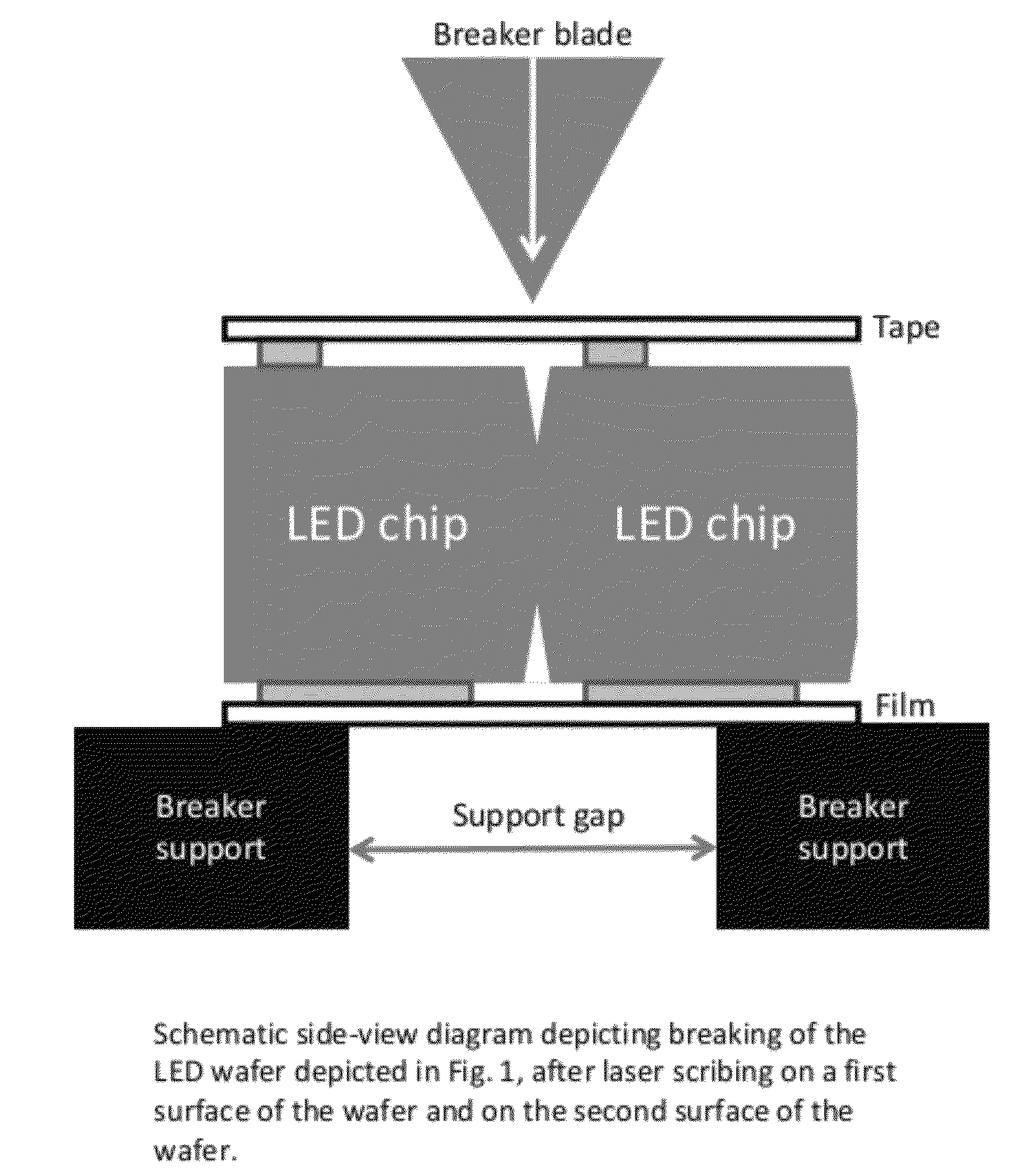
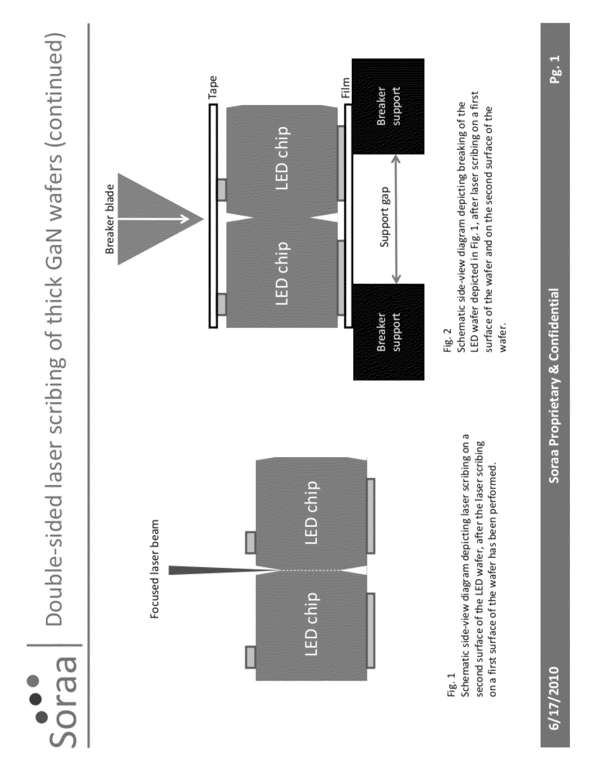
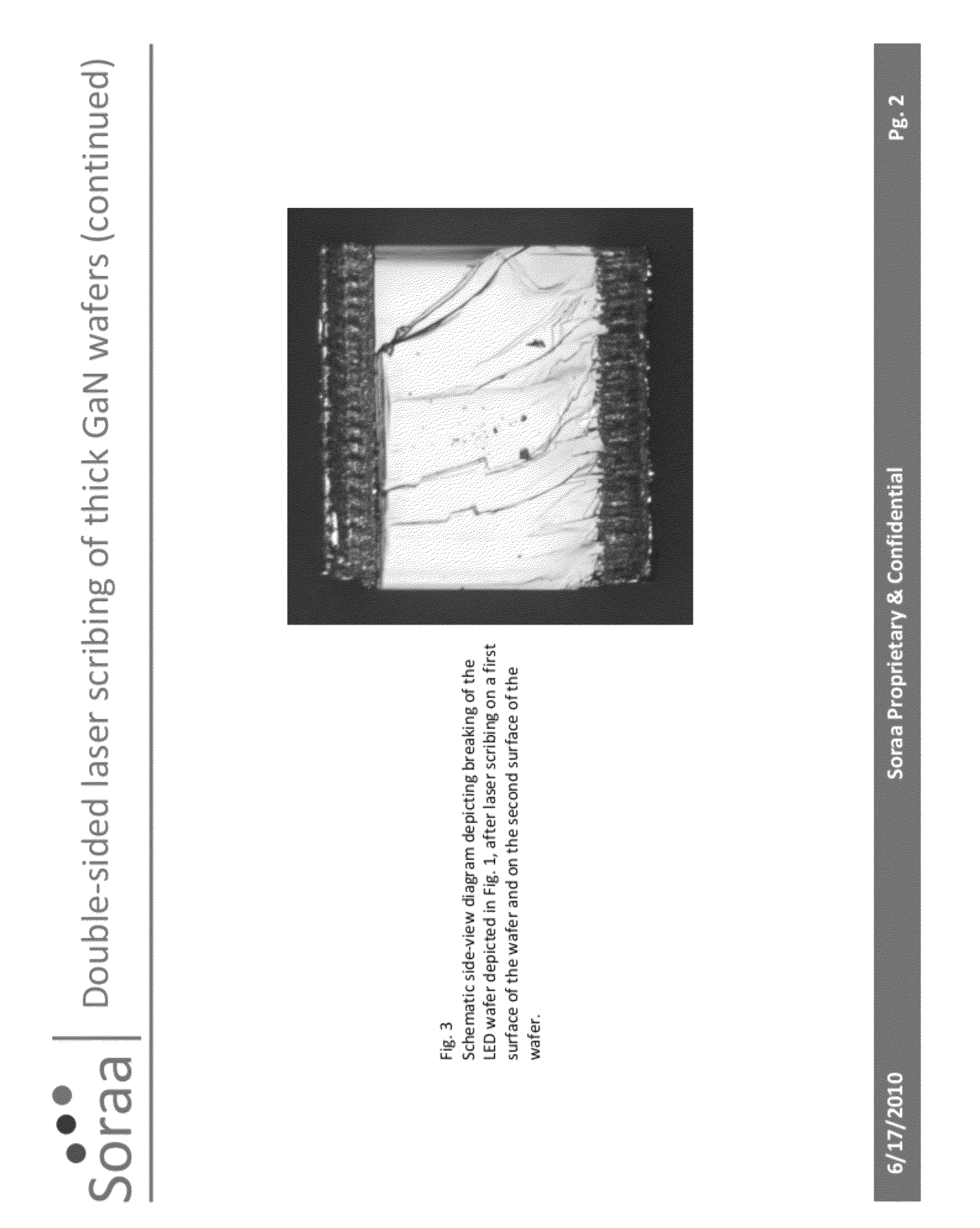
[0016]FIG. 1 is a side-view diagram depicting a laser scribing process for an optical device according to an embodiment of the present invention. In a specific embodiment, the LED wafer is laser-scribed within the ‘scribe streets’ on a first surface of the wafer, along one or more axes according to a specific embodiment. In other embodiments, the scribing can occur using a saw, a diamond scribe, a chemical etchant (with or without a photo-assisted component), reactive ion or plasma etchant or milling, or combinations, and the like. The scribe depth in the scribed regions on the first surface is typically 20-25% of the thickness of the LED wafer according to a specific embodiment. In other embodiments, the scribe depth can vary and have other dimension. In a specific embodiment, the scribe line also has a suitable width and length Of course, there can be other variations, modifications, and alternatives.

[0017]In a specific embodiment, the LED wafer is then flipped over, and is then l...


PUM


Abstract

A method for singulation of thick GaN wafers (e.g., 300-400 um) through the use of a double-side laser-scribe process. In a preferred embodiment, the patterned GaN substrate is processed using a laser-scribe on each side of the substrate to form scribe lines. The scribe lines are aligned to each other. In a preferred embodiment, the substrate has not been subjected to a thinning or polishing process for reducing its thickness.

Description

CROSS REFERENCE TO RELATED APPLICATION[0001]This application claims priority to U.S. Provisional Application No. 61 / 356,478, filed Jun. 18, 2010, which is incorporated herein by reference for all purposes.BACKGROUND OF THE INVENTION[0002]The present invention relates generally to lighting techniques. More specifically, embodiments of the invention include techniques for manufacturing optical devices, such as light emitting diodes (LEDs) using a separation process of thick gallium and nitrogen containing substrates, such as GaN configured in non-polar or semi-polar crystalline orientations. The starting materials can include polar gallium nitride containing materials. The invention can be applied white lighting, multi-colored lighting, general illumination, decorative lighting, automotive and aircraft lamps, street lights, lighting for plant growth, indicator lights, lighting for flat panel displays, and other optoelectronic devices.[0003]In the late 1800's, Thomas Edison invented th...

Claims


Application Information

Patent Timeline
Patent Type & Authority Patents(United States)
IPC IPC(8): H01L21/00
CPCH01L33/0095
Inventor SHARMA, RAJATKATONA, THOMAS M.FELKER, ANDREW
Owner KORRUS INC
Why Eureka
Try Eureka