Variable-gain differential amplifier

a differential amplifier and variable gain technology, applied in the field of integrated circuit amplifiers, can solve the problems of low input impedance, known circuit, 10 k, etc., and achieve the effect of high input impedan

Active Publication Date: 2008-07-15
MICROELECTRONIC INNOVATIONS LLC
View PDF5 Cites 6 Cited by
  • Summary
  • Abstract
  • Description
  • Claims
  • Application Information

AI Technical Summary

Benefits of technology

[0011]In one embodiment, the differential amplifier additionally comprises at least one amplification circuit having a first input coupled to the first output of the first differential circuit and to the second output of the second differential circuit, a second input coupled to the second output of the first differential circuit and to the first output of the second differential circuit, a first output coupled to the first output of the differential amplifier, and a second output coupled to the second output of the differential amplifier. This circuit provides a high open-loop gain and hence allows the bandwidth to be increased. It also allows the gain of the feedback-controlled amplifier to be made more independent of the gain of the first and second differential circuits.
[0012]In one embodiment, the first and second impedances, that provide the negative feedback, are two variable impedances, and the third impedance is a fixed impedance. In actual fact, only one of the first and second impedances need be variable, but the fact that they are both variable provides a symmetry in the design and the operation of the amplifier. This symmetry is advantageous in the case of a differentially controlled system.
[0013]Preferably, the impedances are elements that are essentially resistive which are simpler to produce.
[0015]In one embodiment, the differential amplifier additionally comprises two stabilization circuits in parallel with the amplification circuit connecting, for one, the first output of the first differential circuit and the second output of the second differential circuit to the second output of the differential amplifier and, for the other, the second output of the first differential circuit and the first output of the second differential circuit to the first output of the differential amplifier. These circuits allow for improved stability of the feedback-controlled amplifier.

Problems solved by technology

Whatever the technique used, one drawback of the known circuits is that they exhibit a low input impedance (in the order of 10 kΩ).

Method used


Image

  • Variable-gain differential amplifier
  • Variable-gain differential amplifier
  • Variable-gain differential amplifier

Examples


Embodiment Construction

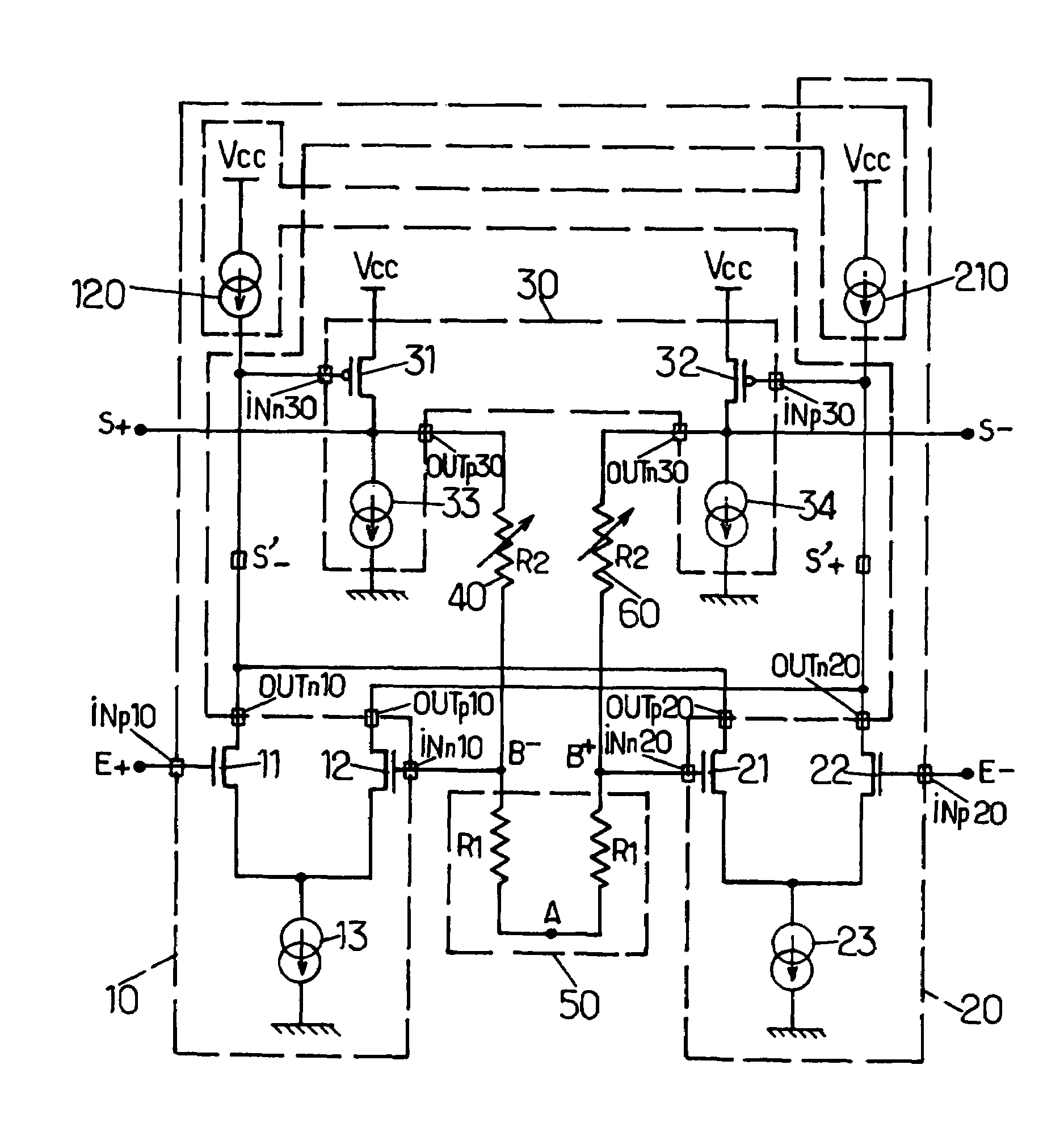
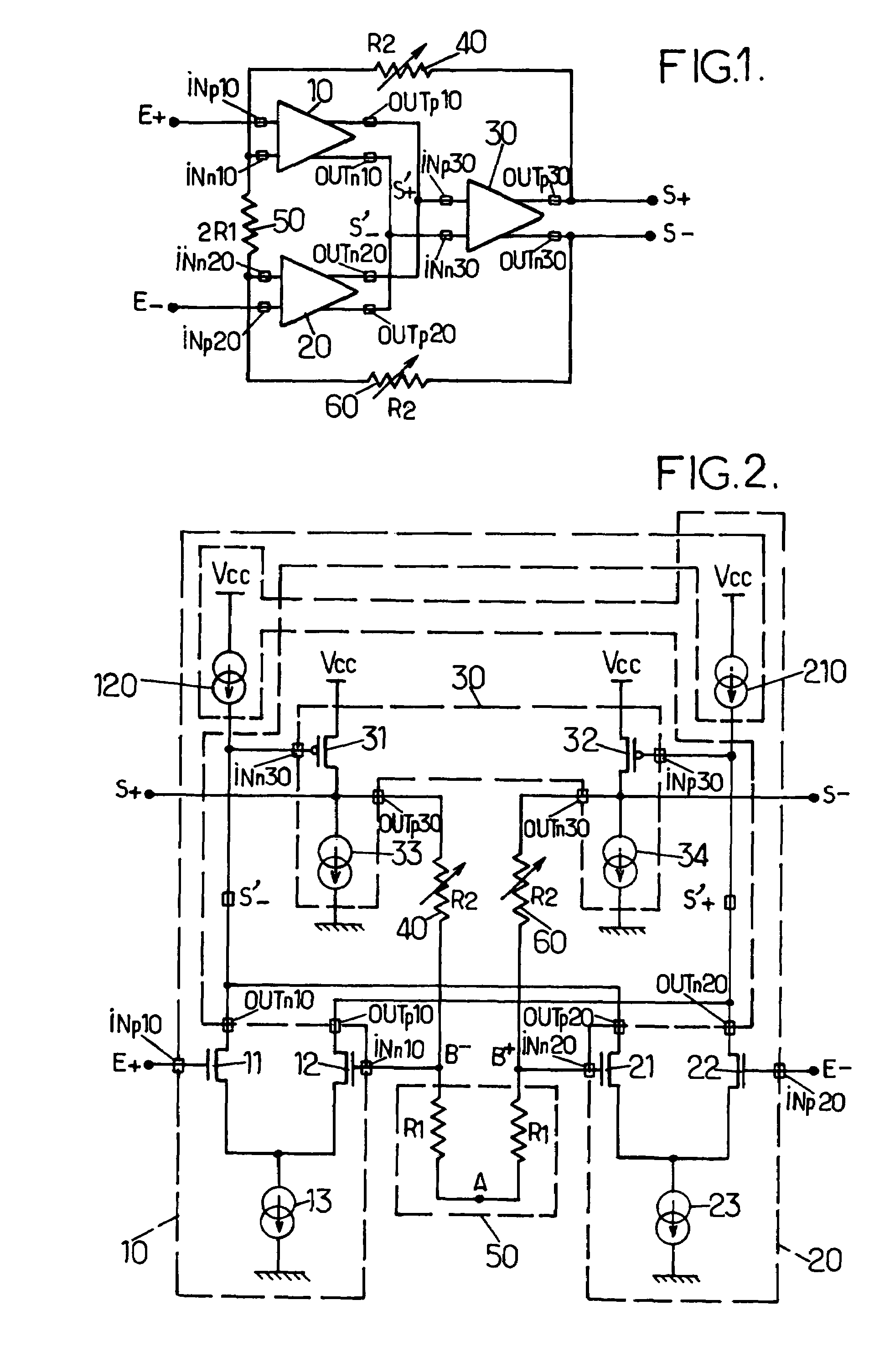
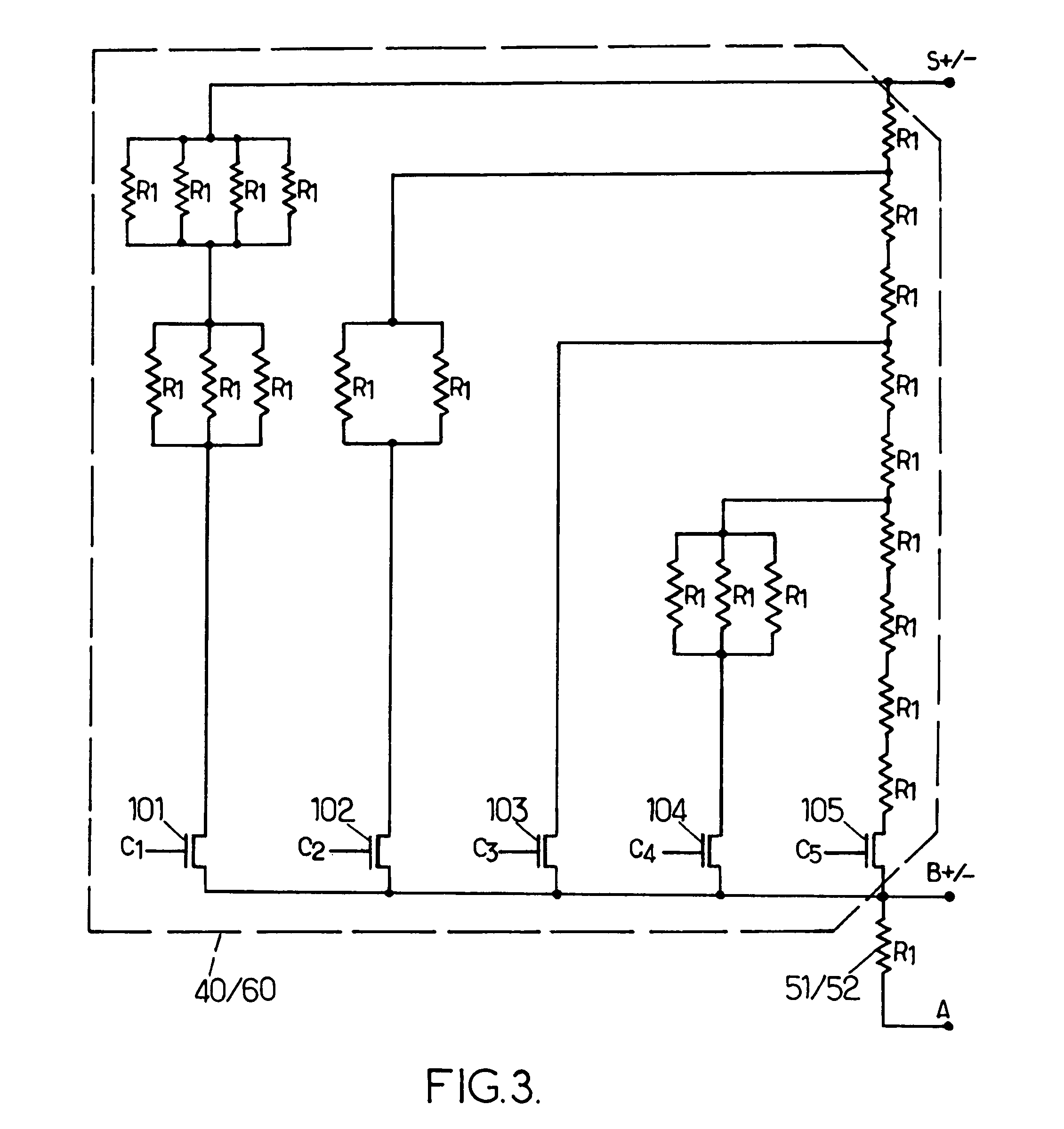
[0026]FIG. 1 is a functional circuit diagram of an exemplary embodiment of a differential amplifier according to the present invention. The amplifier comprises differential amplification circuits 10, 20 and 30, coupled together, in part, via impedances 40, 50 and 60 forming a negative feedback loop for controlling the gain.

[0027]The differential amplification circuits 10 and 20 are preferably identical to one another. Each differential circuit 10 or 20 comprises a positive input INp10 and INp20, respectively, a negative input INn10 and INn20, respectively, a positive output OUTp10 and OUTp20, respectively, and a negative output OUTn10 and OUTn20, respectively. These differential circuits each comprise a differential pair of transistors biased by current sources. The transistors are for example MOSFET transistors. Such differential circuits are high-gain circuits with a high input impedance. The positive input of the differential circuit 10 is connected to a positive input terminal E...


PUM


Abstract

A variable-gain amplifier with high input impedance includes positive and negative inputs, positive and negative outputs, first and second differential circuits and first, second and third impedances. The impedances form an impedance bridge between the outputs. The first and second differential circuits each have one input coupled to one of the inputs of the differential amplifier, one input coupled to the impedance bridge, and two outputs connected to the outputs of the differential amplifier. At least one of the impedances is a variable impedance.

Description

RELATED APPLICATION[0001]This application claims priority of French Patent Application No. 05 03820, filed Apr. 15, 2005, which is incorporated herein in its entirety by this reference.[0002]1. Field of the Invention[0003]The invention relates to integrated circuit amplifiers and, more particularly, to differential amplifiers having a gain control input for adjusting the amplification ratio.[0004]2. Background of the Invention[0005]Variable-gain amplifiers are notably used in Automatic Gain Control (AGC) amplification circuits, in particular in audio applications.[0006]Among the many known types of variable-gain amplifiers, differential amplifiers use pairs of signals called differential signals. Differential signals allow the signal-to-noise ratio to be improved and are capable of working at higher frequencies. Such amplifiers are, for example, used in data transmission systems.[0007]Essentially, two techniques are used in the design of variable-gain amplifiers. A first technique i...

Claims


Application Information

Patent Timeline
Patent Type & Authority Patents(United States)
IPC IPC(8): H03F3/45
CPCH03F3/45475
Inventor GATTI, PAOLO
Owner MICROELECTRONIC INNOVATIONS LLC
Why Eureka
Try Eureka