Optical modulator and optical transmitter

a technology of optical modulator and optical transmitter, which is applied in the direction of instruments, non-linear optics, optics, etc., can solve the problems of limited bandwidth improvement, certain amount of inverse modulation, and difficulty in high-speed modulation, so as to improve the modulation bandwidth and speed. the effect of speeding up the rate and widening the modulation bandwidth

Active Publication Date: 2008-07-15
FUJITSU LTD
View PDF8 Cites 4 Cited by
  • Summary
  • Abstract
  • Description
  • Claims
  • Application Information

AI Technical Summary

Benefits of technology

[0015]In an optical modulator of the abovementioned configuration, the loss with respect to the high frequency component of the electrical signal in the second region on the output side of the interaction section is made relatively greater than the loss with respect to the high frequency component of the electrical signal in the first region on the input side of the interaction section. As a result the inverse modulation in the high frequency band in the second region where the modulation direction is reversed to that of the first region is suppressed more than for a conventional optical modulator which uses inverse modulation. Therefore a wider modulation bandwidth is realized.
[0016]Furthermore, the optical transmitter of the present invention, uses the abovementioned optical modulator to externally modulate and transmit an outgoing beam from a light source. In such an optical transmitter, modulated signal light can be transmitted to the outside at a faster rate.
[0017]According to the optical modulator of the present invention as described above, by making the loss of the second region with respect to the high frequency component of the electrical signal propagated through the signal electrode relatively large, the modulation band in the overall optical modulator can be made a wider band, and modulation at a higher speed than heretofore is possible. According to the optical transmitter which uses such an optical modulator, optical signals having a wider bandwidth can be transmitted, and hence a characteristic improvement of the error rate and the like on the reception side becomes possible.

Problems solved by technology

Therefore there is a problem in that the modulation band width is limited, so that high speed modulation becomes difficult.
However, in the conventional technology which gives a wider band width by using the above inverse modulation, since the modulation component of the high frequency band in the polarization inversed region (inverse modulation section) has not become small enough, then in the high frequency band, a certain amount of inverse modulation occurs.
Therefore there is a problem in that the amount of improvement in bandwidth is limited.
Furthermore, in the conventional technology for improving the response characteristics by changing the electrode width of the signal electrode and the ground electrode along the light propagation direction, the influence on the light due to the resonance of the generated acoustic wave attributable to the piezoelectricity of the substrate can be reduced, but an increase in the propagation loss of the electrical signal in the high frequency as mentioned above cannot be effectively suppressed.
Therefore there is the problem that it is difficult to realize a wider band width.

Method used


Image

  • Optical modulator and optical transmitter
  • Optical modulator and optical transmitter
  • Optical modulator and optical transmitter

Examples


first embodiment

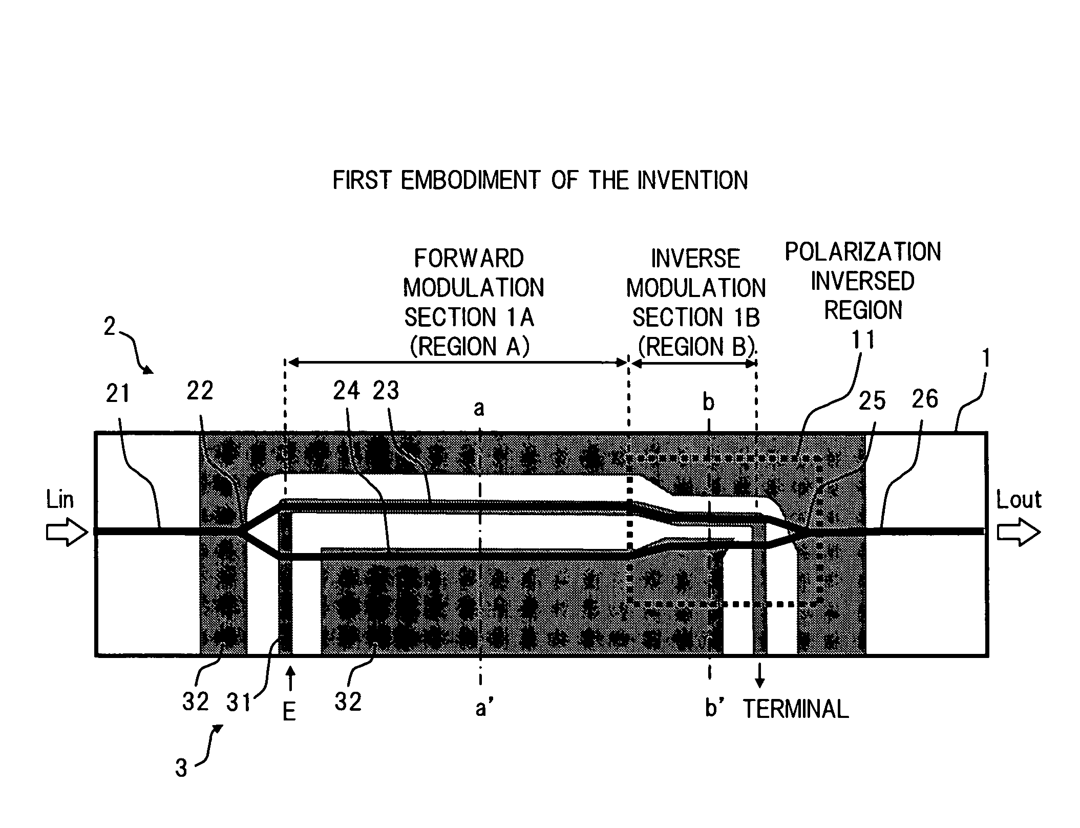
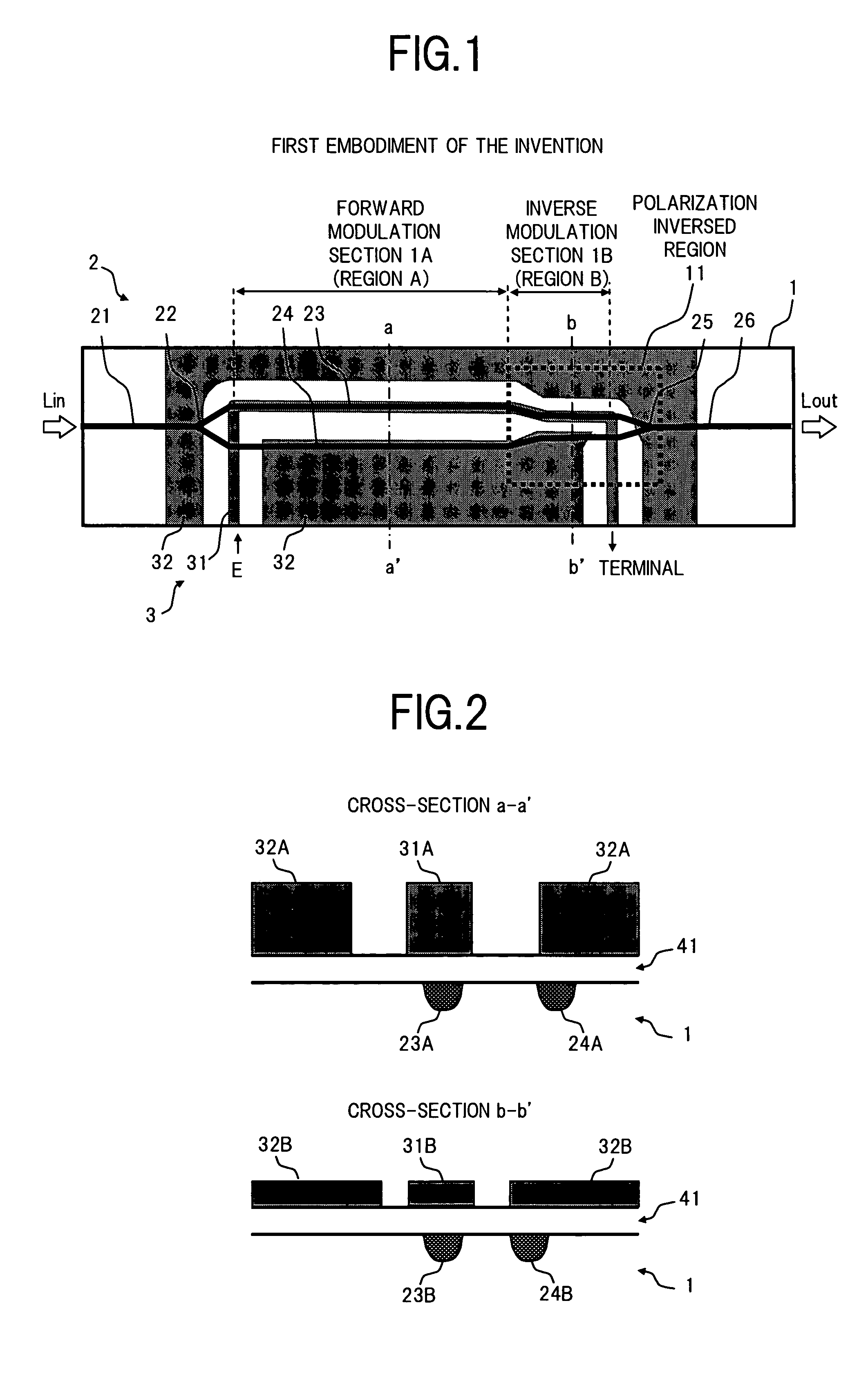
[0049]FIG. 1 is a plan view showing a configuration of an optical modulator according to the present invention. Moreover, FIG. 2 is an enlarged view of section a-a′ and section b-b′ in the optical modulator of FIG. 1.

[0050]In FIG. 1 and FIG. 2, the optical modulator of the first embodiment comprises for example a substrate 1 having an electro-optic effect, an optical waveguide 2 of a Mach-Zehnder type formed on the substrate 1, and an electrode 3 formed on the surface of the substrate 1.

[0051]The substrate 1 uses a crystal substrate of for example Z-cut lithium niobate (LiNbO3) or Lithium Tantalate (LiTaO2), and in a region (hereunder interaction section) where light propagated through the optical waveguide 2 and an electric signal E propagated through the electrode 3 interact, a first region A on the input side which spans from the light input end over a predetermined length in the longitudinal direction (the light propagation direction) is made a forward modulation section 1A, and...

second embodiment

[0069]Next is a description of the present invention.

[0070]FIG. 9 shows an enlarged cross-section of respective sections in an optical modulator according to the second embodiment of the present invention. The plan view showing the configuration of the overall optical modulator of the second embodiment is similar to the case of the first embodiment shown in FIG. 1. Therefore, illustration is omitted here.

[0071]The optical modulator of the second embodiment is one where, for a buffer layer 41 formed between the surface of the substrate 1 and the signal electrode and the ground electrode, so that the dielectric loss of a buffer layer 41B (refer to the bottom of FIG. 9) positioned on the inverse modulation section 1B is greater than the dielectric loss of a buffer layer 41A (refer to the top of FIG. 9) positioned on the forward modulation section 1A, the substance constituting the respective buffer layers 41A and 41B is made different. The configuration other than for the buffer layers...

third embodiment

[0079]Next is a description of the present invention.

[0080]FIG. 12 is a plan view showing a configuration of an optical modulator according to the third embodiment of the present invention. Moreover, FIG. 13 is an enlarged view of section a-a′ and section b-b′ in the optical modulator of FIG. 12.

[0081]In FIG. 12 and FIG. 13, the point where the configuration of the optical modulator the third embodiment is significantly different to the configuration of the first embodiment shown in FIG. 1 and FIG. 2 is that regarding the distance (electrode spacing) between the signal electrode 31 and the ground electrode 32, the electrode spacing in the inverse modulation section 1B is relatively greater than the electrode spacing in the forward modulation section 1A. Furthermore, since the impedance increases if the electrode spacing is relatively increased, then by making the sectional area of the signal electrode 31B and the ground electrode 32B in the inverse modulation section 1B (the bottom ...


PUM

PropertyMeasurementUnit
thicknessaaaaaaaaaa
electric fieldaaaaaaaaaa
electrical lossaaaaaaaaaa

Abstract

In an optical modulator of the invention, a signal electrode and a ground electrode are formed along a pair of branching waveguides of a Mach-Zehnder type optical waveguide, and a first region positioned on an input side of an interaction section of light and an electric signal is made a forward modulation section, and a second region positioned on an output side is made an inverse modulation section, and a spacing or the like of the signal electrode and the ground electrode is optimized so that that a loss produced in the second region is relatively greater than a loss produced in the first region, with respect to a high frequency component of an electric signal propagated through the signal electrode. As a result a wider modulation bandwidth can be realized.

Description

BACKGROUND OF THE INVENTION [0001]1. Field of the Invention[0002]The present invention relates to an optical modulator and an optical transmitter used for optical transmission, and in particular relates to an optical modulator of a waveguide type which modulates light using an electro-optic effect, and to an optical transmitter which uses this.[0003]2. Description of the Related Art[0004]For example, an optical waveguide device which uses an electro-optic crystal such as lithium niobate (LiNbO3), lithium tantalate (LiTaO2) or the like, is manufactured by forming a metal film on a part of a crystal substrate and thermal diffusing, or by proton exchanging in benzoic acid after patterning, to thereby form an optical waveguide, and afterwards providing electrodes in the vicinity of the optical waveguide. As one optical waveguide device which uses an electro-optic crystal, there is known an optical modulator as shown for example in FIG. 28.[0005]In general, the optical modulator, dependi...

Claims


Application Information

Patent Timeline
Patent Type & Authority Patents(United States)
IPC IPC(8): G02F1/035
CPCG02F1/0356G02F1/2255G02F2203/25G02F2201/122
Inventor SUGIYAMA, MASAKI
Owner FUJITSU LTD
Why Eureka
Try Eureka