Metamaterial modulator
A technology of modulators and metamaterials, applied in the direction of instruments, antennas, electrical components, etc., can solve the problems of unrealistic application and poor modulation effect, and achieve the effects of ultra-high modulation effect, wide modulation bandwidth, and high modulation depth
- Summary
- Abstract
- Description
- Claims
- Application Information
AI Technical Summary
Problems solved by technology
Method used
Image
Examples
Embodiment 1
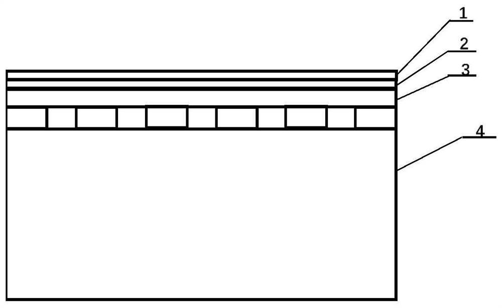
[0047] figure 1Shown is a schematic structural diagram of a metamaterial modulator, an embodiment of the present invention provides a metamaterial modulator, the metamaterial modulator includes a surface layer 1, a graphene layer 2, and a flexible dielectric layer 3 arranged from top to bottom , silicon rectangular strip structure substrate layer 4;
[0048] Among them, the flexible dielectric layer 3 is attached to the upper surface of the silicon rectangular structure substrate layer 4 , the graphene layer 2 is attached to the upper surface of the flexible dielectric layer 3 , and the surface layer 1 is attached to the upper surface of the graphene layer 2 .
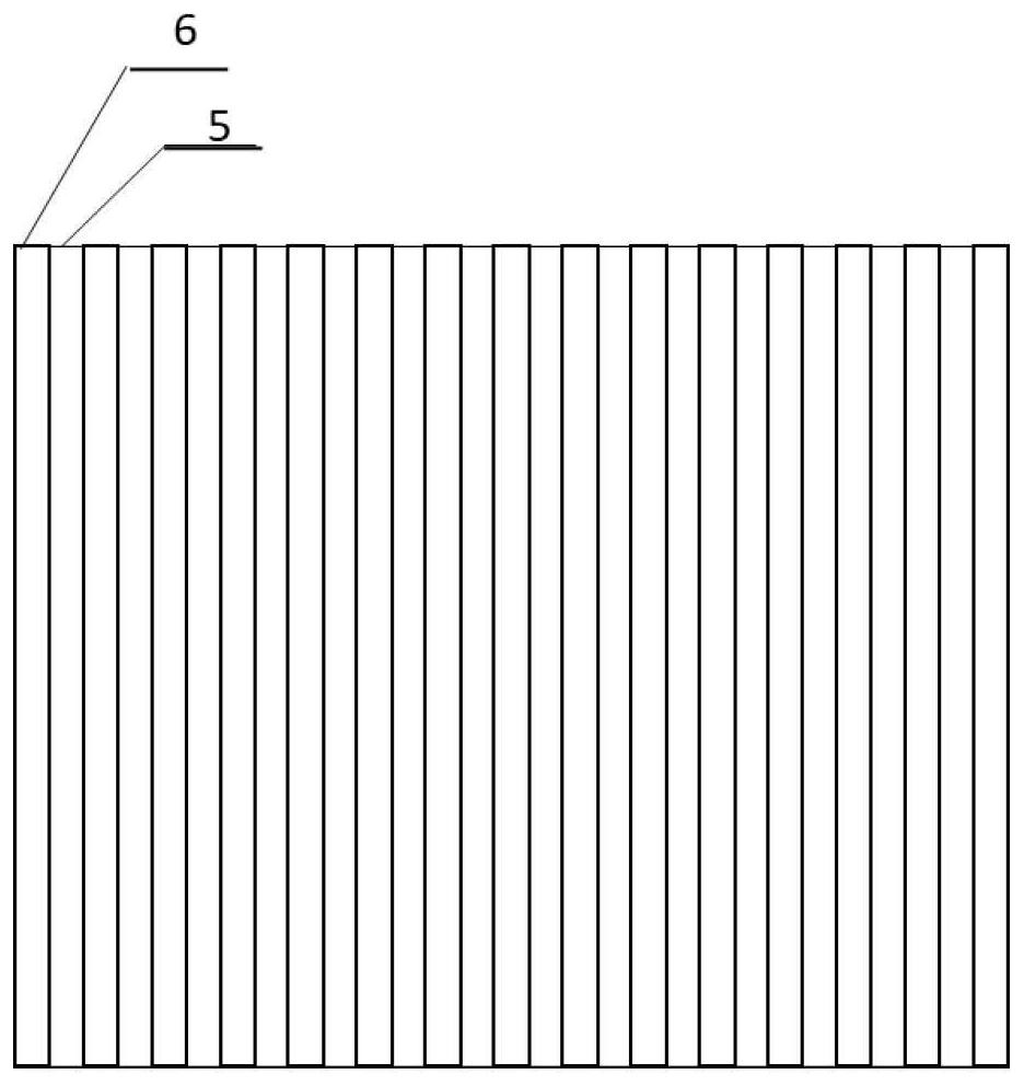
[0049] figure 2 Shown is a schematic diagram of a silicon strip structure of a metamaterial modulator, and the silicon strip structure substrate layer 4 is composed of several identical silicon strip structures arranged alternately.
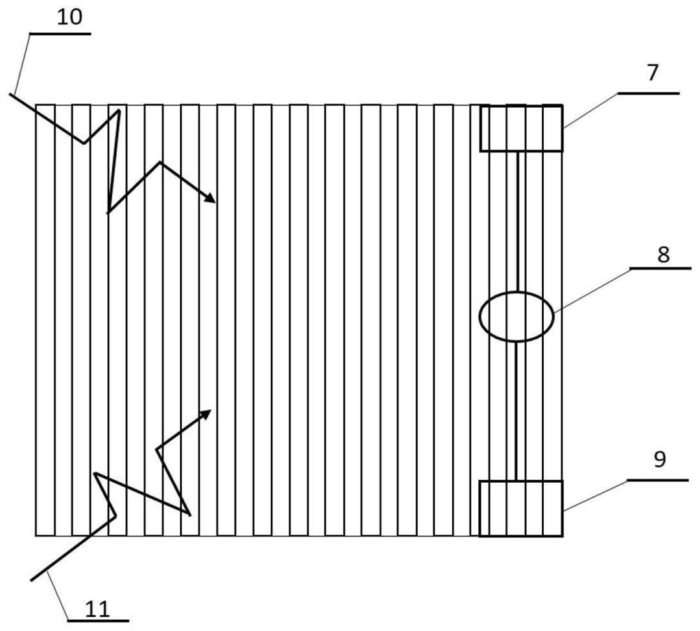
[0050] image 3 Shown is the electrode distribution diagram of a metamaterial mod...
Embodiment 2
[0067] Image 6 Shown is a flow chart of a method for preparing a metamaterial modulator, an embodiment of the present invention provides a method for preparing a metamaterial modulator, and the method includes:
[0068] S1. Prepare a layer of high-resistance silicon layer as the underlying substrate layer 4 .
[0069] Prepare a 300 μm thick high-resistance silicon layer.
[0070] S2. Etching a silicon strip structure with a height of 65 microns on the underlying substrate layer 4 .
[0071] S3. Spin-coating polyimide on the substrate layer 4 with the rectangular silicon strip structure, the specific steps include. :
[0072] Spin-coat 10 μm thick polyimide film on 300 μm high-resistance silicon: After cleaning the prepared high-resistance silicon, spin-coat a polyimide solution with a viscosity of 3600 (centipoise) on the silicon structure surface, spin-coating time For 60 seconds, the speed is 2200RPM. Then the polyimide solution is baked, the baking temperature is 120°...
PUM
| Property | Measurement | Unit |
|---|---|---|
| Thickness | aaaaa | aaaaa |
Abstract
Description
Claims
Application Information


