Word line voltage boosting circuit and a memory array incorporating same

a voltage boosting circuit and word line technology, applied in static storage, digital storage, instruments, etc., can solve the problems of occupying precious die area reducing the voltage of word lines, etc., and achieve the effect of boosting the voltage and boosting the voltage on the word lines

Active Publication Date: 2008-07-22
SILICON STORAGE TECHNOLOGY
View PDF14 Cites 42 Cited by
  • Summary
  • Abstract
  • Description
  • Claims
  • Application Information

AI Technical Summary

Benefits of technology

[0009]Accordingly, in the present invention, two embodiments of a word line voltage boosting circuit and memory arrays incorporating such circuits are disclosed. In the first embodiment an array of non-volatile memory cells comprises a semiconductor substrate of a first conductivity type. The array comprises a first group of non-volatile memory cells. Each memory cell comprises a first region of a second conductivity type in the substrate, and a second region of the second conductivity type in the substrate, spaced apart from the first region, thereby defining a channel region therebetween. A floating gate is insulated from a first portion of the channel region for controlling the conduction of current in the first portion of the channel region. A control gate is adjacent to and spaced apart from the floating gate, and is insulated from a second portion of the channel region for controlling the conduction of current in the second portion of the channel region. A first word line electrically connects all the control gates of all the cells in the same row in the first group. The array further comprises a second group of non-volatile memory cells, each of which is similar to the cells from the first group. A second word line electrically connects all the control gates of all the cells in the same row in the second group. The first word line forms a capacitor with the second word line. A first switch is connected to the first word line and is for electrically connecting the first word line to a first voltage source. A second switch is connected to the second word line for electrically connecting the second word line to a second voltage source. A sequencing circuit activates the first switch connecting the first word line to the first voltage source, while maintaining the second switch in a position to disconnect the second word line from the second voltage source; and activates the second switch connecting the second word line to the second voltage source, while maintaining the first switch in a position to disconnect the first word line from the first voltage source. The alternate switching of the first switch and the second switch boosts the voltage on the first word line.
[0010]In a second embodiment, an array of non-volatile memory cells comprises a semiconductor substrate of a first conductivity type. A group of non-volatile memory cells are formed with each cell comprising a first region of a second conductivity type in the substrate. Each cell further comprises a second region of the second conductivity type in the substrate, spaced apart from the first region, thereby defining a channel region therebetween. A floating gate is insulated from a first portion of the channel region for controlling the conduction of current in the first portion of the channel region. A control gate is adjacent to and spaced apart from the floating gate, and is insulated from a second portion of the channel region for controlling the conduction of current in the second portion of the channel region. A word line electrically connects all the control gates of all the cells in the same row in the group. A switch is connected to the word line for electrically connecting the word line to a first voltage source. A capacitor has a first end and a second end, with the first end electrically connected to the word line, and with the second end electrically connected to a second voltage source. A sequencing circuit activates the switch connecting the word line to the first voltage source, while disconnecting the second end of the capacitor from the second voltage source; and connects the second end of the capacitor to the second voltage source, while maintaining the first switch in a position to disconnect the word line from the first voltage source. The alternate switching of the switch boosts the voltage on the word line.

Problems solved by technology

The weakly erased cells can cause yield loss, data retention, and cycling problems.
However, redundant rows or sectors is costly in that they occupy precious die area.
In addition, they may not be enough if the failure rate of weakly erased cells is high.
This “solution,” however, takes longer time.
This has the disadvantage of reducing the size of the memory that is available for usage.

Method used


Image

  • Word line voltage boosting circuit and a memory array incorporating same
  • Word line voltage boosting circuit and a memory array incorporating same
  • Word line voltage boosting circuit and a memory array incorporating same

Examples


first embodiment

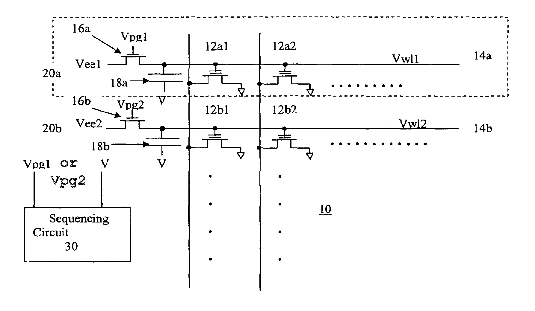
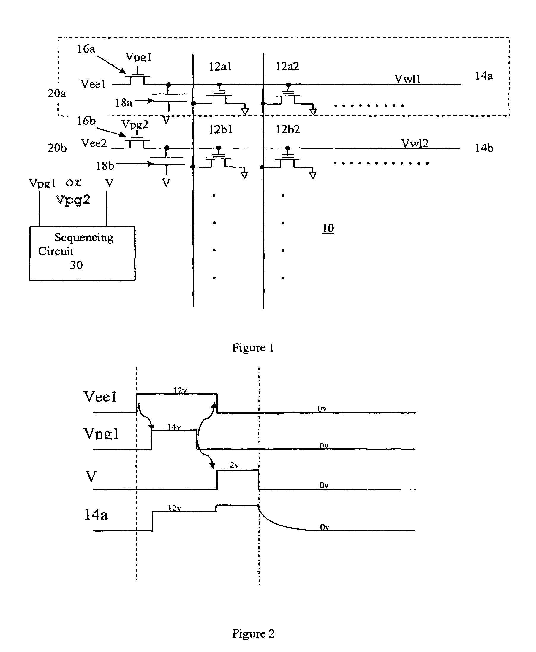
[0017]Referring to FIG. 1 there is shown a schematic circuit diagram of a non volatile memory array 10 of the present invention with an improved wood line voltage boosting circuit of the present invention. As discussed in the background of the invention and as discussed in U.S. Pat. Nos. 5,029,130 and 5,572,054, (whose disclosures are incorporated herein in their entirety), the array 10 comprises a plurality of memory cells, such as memory cell 12a1, 12a2, 12b1, and 12b2, arranged in a plurality of rows (e.g. rows 20a and 20b) and columns. Further, as well known in the art, the term “row” and “column” may be inter used interchangeably. In the preferred embodiment, each of the memory cells 12a1, 12a2, 12b1, and 12b2, is of the type disclosed in U.S. Pat. Nos. 5,029,130 and 5,572,054 in which the memory cell is a split gate floating gate type cell. A cross-sectional view of the memory cell 12 is shown in FIG. 6. The semiconductor substrate 80 in which these memory cells 12 are formed ...

second embodiment

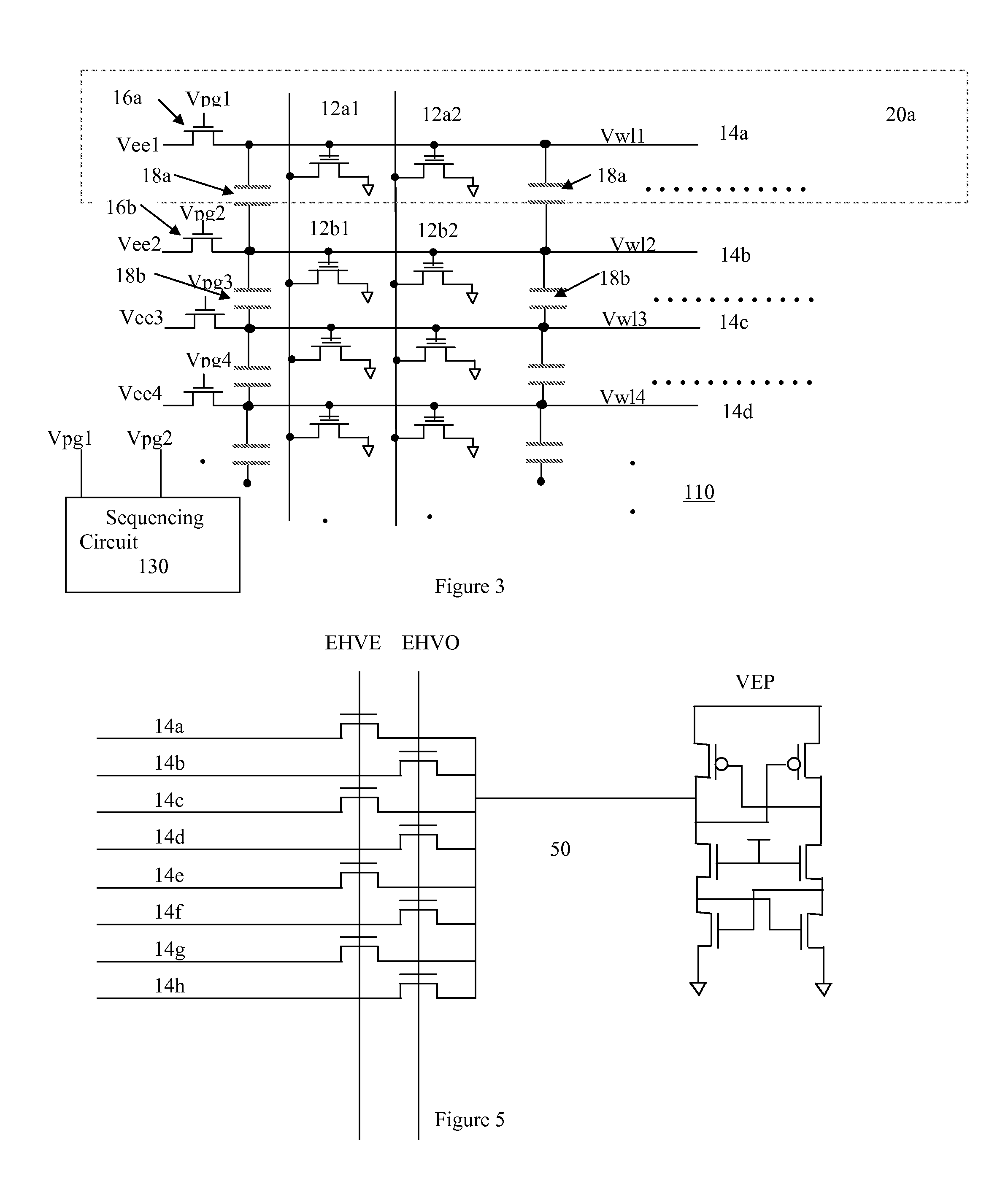
[0023]Referring to FIG. 3, there is shown a memory array 110 of the present invention. The memory array 110 is similar to the memory array 10 in that it has a plurality memory cells 12 (such as memory cells 12a1, 12a2, 12b1, and 12b), arrange in a plurality of rows 20 such as row 20a and a plurality of columns. Each of the memory cells 12 arranged in the same row 20 are connected by a common word line 14, such as word line 14a, 14b, 14c and 14d. The word lines 14a, 14b, 14c and 14d are also designated as Vwl1, Vwl2, Vwl3 and Vwl4, respectively. The word line 14a or Vwl1 is connected to erase voltage Vee1 through a switching transistor 16a. Similarly, the word line 14b or Vwl2 is connected to erase voltage Vee2 through a switching transistor 16b. The word line 14c or Vwl3 is connected to erase voltage Vee3 through a switching transistor 16c, while the word line 14d or Vwl4 is connected to erase voltage Vee4 through a switching transistor 16d. Each of the switching transistors 16a, 16...


PUM


Abstract

A first embodiment of a word line voltage boosting circuit for use with an array of non-volatile memory cells has a capacitor, having two ends, connected to the word line. One end of the capacitor is electrically connected to the word line. The other end of the capacitor is electrically connected to a first voltage source. The word line is also connected through a switch to a second source voltage source. A sequencing circuit activates the switch such that the word line is connected to the second voltage source, and the other end of the capacitor is not connected to the first voltage source. Then the sequencing circuit causes the switch to disconnect the word line from the second voltage source, and connect the second end of the capacitor to the first voltage source. The alternate switching of the connection boosts the voltage on the word line. In a second embodiment, a first word line is electrically connected to a first switch to a first voltage source. An adjacent word line, capacitively coupled to the first word line, is electrically connected to a second switch to a second voltage source. A sequencing circuit activates the first switch and the second switch such that the first word line is connected to the first voltage source, and the second word line is disconnected from the second voltage source. Then the sequencing circuit causes the first switch to disconnect the first word line from the first voltage source, and causes the second word line to be electrically connected to the second voltage source. The alternate switching of the connection boosts the voltage on the first word line, caused by its capacitive coupling to the second word line. A boosted voltage on the word line may be used to improve cycling and yield, where the memory cells of the array are of the floating gate type and erase through the mechanism of Fowler-Nordheim tunneling from the floating gate to a control gate which is connected to the word line.

Description

TECHNICAL FIELD[0001]The present invention relates to a word line boosting circuit for boosting the voltage supplied on a word line in an array of non-volatile memory cells, wherein voltage may be used by the cell to erase, and more particularly wherein the voltage is boosted through the use of either an additional capacitor, or wherein the voltage is self boosted by the capacitance from an adjacent word line.BACKGROUND OF THE INVENTION[0002]Non-volatile memory integrated circuit chips are well known in the art. One type of a non-volatile memory cell is of a split gate type, see for example U.S. Pat. Nos. 5,029,130 and 5,572,054, whose disclosures are incorporated herein in their entirety. In these references, each memory cell is a split gate floating gate type cell. A semiconductor substrate is of a first conductivity type. A cell has a first region in the substrate of a second conductivity type. The cell further has a second region in the substrate of the second conductivity type,...

Claims


Application Information

Patent Timeline
Patent Type & Authority Patents(United States)
IPC IPC(8): G11C11/34
CPCG11C16/08G11C8/08
Inventor LIN, YA-FENLIN, ELBERTTRAN, HIEU VANFRAYER, JACK EDWARDCHEN, BOMY
Owner SILICON STORAGE TECHNOLOGY
Why Eureka
Try Eureka