Fast trigger ESD device for protection of integrated circuits

a technology of integrated circuits and triggers, applied in the direction of circuit arrangements, electrical apparatus, and circuit arrangements responsive to excess voltage, can solve the problems of critical protection of gate dielectrics from esd damage, damage to the gate oxide of a mos device, and the dielectrics that are susceptible to esd induced damag

Active Publication Date: 2008-08-05
ALTERA CORP
View PDF24 Cites 25 Cited by
  • Summary
  • Abstract
  • Description
  • Claims
  • Application Information

AI Technical Summary

Benefits of technology

[0008]The simultaneous turning on of the PNP and NPN bipolar transistors allows the SCR to be turned on rapidly in an ESD event. The trigger and holding voltages of the ESD device can also be very low (<2.5V). Thus, the ESD device can be used for any core circuits such as PLL o

Problems solved by technology

Many MOS devices include thin gate dielectrics that are susceptible to ESD induced damage.
Therefore, protecting gate dielectrics from ESD damage is critical.
It is well known that ESD, especially the Charge-Device Model (CDM) type of ESD, can damage the gate oxide of a MOS device.
Although ESD devices can be used to protect the gate oxide, oxide rupture can still occur if t

Method used


Image

  • Fast trigger ESD device for protection of integrated circuits
  • Fast trigger ESD device for protection of integrated circuits
  • Fast trigger ESD device for protection of integrated circuits

Examples


Embodiment Construction

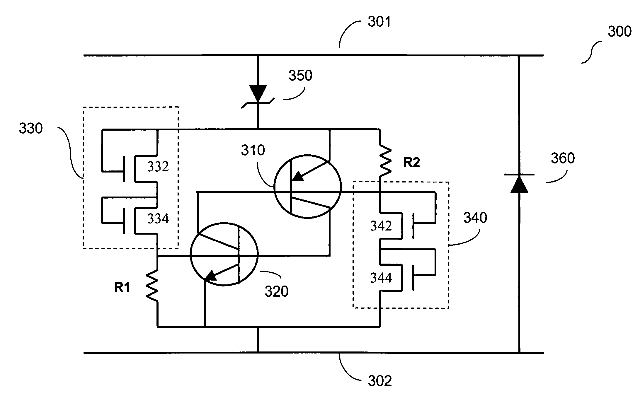
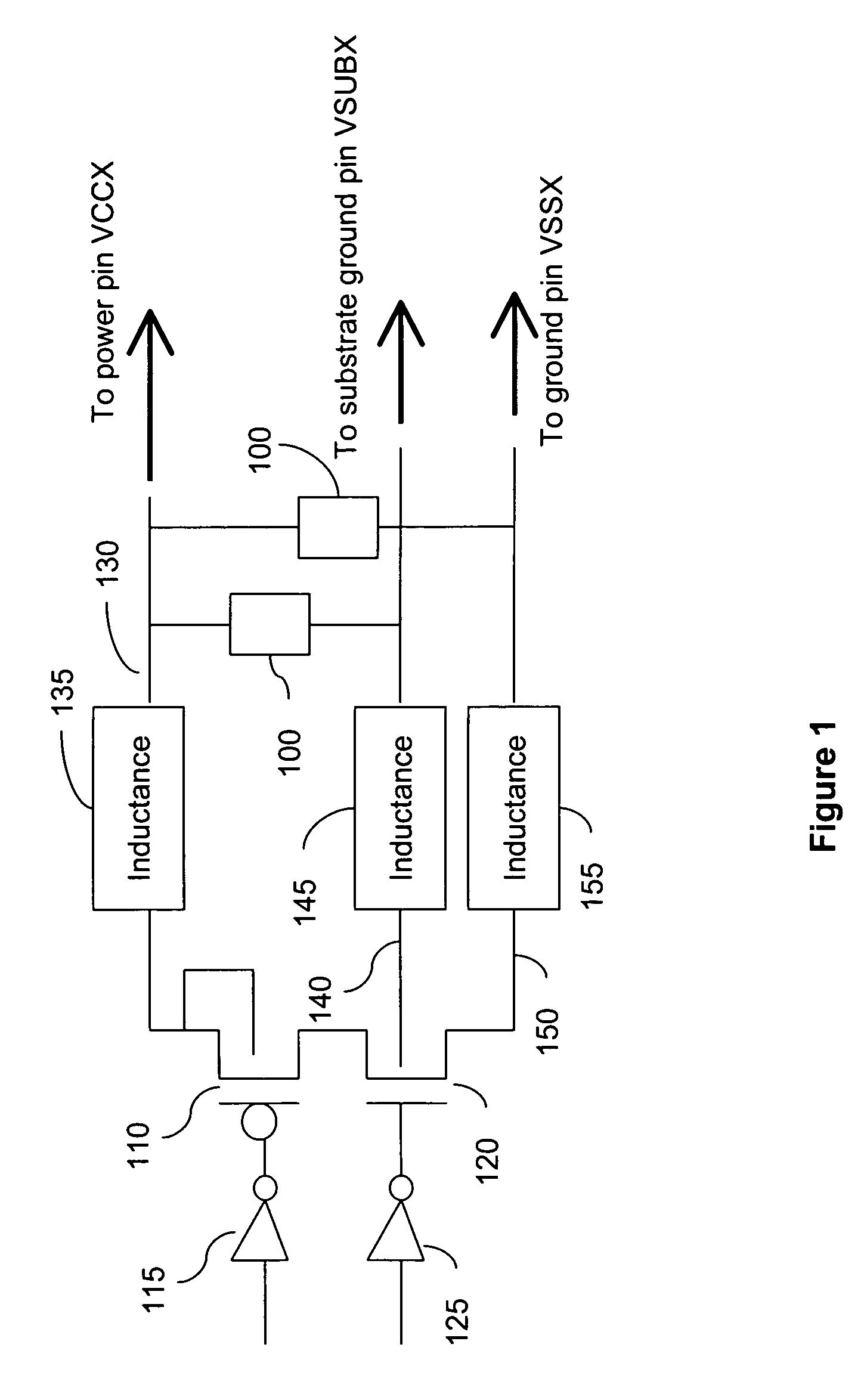
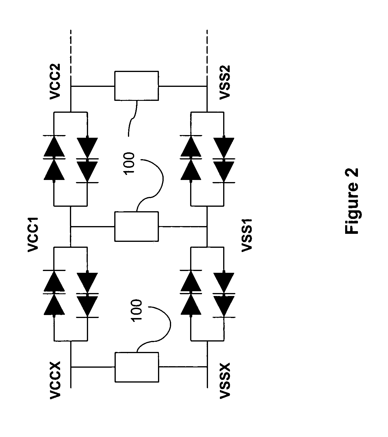
[0016]The present invention provides a fast trigger ESD device with a low trigger voltage. To illustrate the need for such an ESD device, FIG. 1 depicts a pair of complimentary MOS (CMOS) transistors, which include a P-type MOS (PMOS) transistor 110 and an N-type MOS (NMOS) transistor 120, in an integrated circuit. The gates of transistors 110 and 120 are connected to internal circuits (not shown) of the integrated circuit through inverters 115 and 125, respectively. The source and substrate of PMOS transistor 110 is connected to a power pin or bus VCCX via an interconnect line 130. The substrate of NMOS transistor 120 is connected to a substrate ground pin or bus VSUBX via an interconnect line 140. The source of NMOS transistor 120 is connected to a general ground pin or bus VSSX via an interconnect line 150. Interconnect lines 130, 140, and 150 usually contribute parasitic inductance 135, 145, and 155, respectively. Parasitic inductance 135, 145, and 155 may also include contribut...


PUM


Abstract

The present invention provides an ESD device for protecting thin oxide layers in transistors or capacitors in an integrated circuit. In one embodiment, the ESD device includes a silicon-controlled rectifier (SCR), the SCR including a PNP bipolar transistor and a NPN bipolar transistor. The ESD device further includes first and second trigger devices coupled to the SCR and configured to simultaneously turn on the PNP bipolar transistor and the NPN bipolar transistor in response to an ESD pulse on the ESD device. The base of the NPN bipolar transistor is floating to allow a first external resistor to be connected between the base and emitter of the NPN bipolar transistor. A second external resistor can be connected between the base and emitter of the PNP bipolar transistor.

Description

BACKGROUND[0001]The present invention relates to electronic devices, and more specifically to electrostatic discharge (ESD) protection of integrated circuits.[0002]Metal-oxide-semiconductor (MOS) devices, such as MOS transistors and MOS capacitors are important components in integrated circuits. Many MOS devices include thin gate dielectrics that are susceptible to ESD induced damage. As the thickness of gate dielectrics scales down in more advanced technologies, the gate dielectrics, such as gate oxide, can rupture at lower voltages. Therefore, protecting gate dielectrics from ESD damage is critical.[0003]It is well known that ESD, especially the Charge-Device Model (CDM) type of ESD, can damage the gate oxide of a MOS device. Although ESD devices can be used to protect the gate oxide, oxide rupture can still occur if the ESD devices have higher trigger voltages than the oxide breakdown voltage. Even when the trigger voltages of the ESD devices are lower than the oxide breakdown vo...

Claims


Application Information

Patent Timeline
IPC IPC(8): H02H3/20
CPCH01L27/0262
Inventor O, HUGH SUNG-KISHIH, CHIH-CHINGLIU, YOW-JUANG BILLHUANG, CHENG-HSIUNGWU, WEI-GUANGKWONG, BILLY JOW-TAIGAO, YU-CHENG RICHARD
Owner ALTERA CORP
Why Eureka
Try Eureka