System and method for providing a dual via architecture for thin film resistors

a thin film resistor and via architecture technology, applied in the field of semiconductor technology, can solve the problems of incompatible resist masks with many of the etchants, too thin stringers to survive the conductor dry etch process, and inability to meet the requirements of many etchants, and achieve the effect of efficient manufacturing of thin film resistor apparatus

Active Publication Date: 2008-08-12
NAT SEMICON CORP
View PDF4 Cites 38 Cited by
  • Summary
  • Abstract
  • Description
  • Claims
  • Application Information

AI Technical Summary

Benefits of technology

[0007]To address the above-discussed deficiencies of the prior art, it is a primary object of the present invention to provide a system and method for efficiently manufacturing a thin film resistor apparatus in an integrated circuit.
[0015]By separately performing (1) the via etch process for the vias that connect to the ends of the thin film resistor, and (2) the via etch process for the at least one substrate via, the thickness of the resistor protect layer that is placed over the thin film resistor may be minimized. This enables the wet etch time for resistor protect layer to be decreased. This means that there will be less etch undercut of the resistor protect layer, less variability in the length of the thin film resistor, and less variability in resistor matching.
[0016]It is an object of the present invention to provide a method for efficiently manufacturing a thin film resistor apparatus in an integrated circuit.
[0017]It is also an object of the present invention to provide a method for efficiently providing a resistor protect layer to protect a thin film resistor during the steps of a manufacturing process.
[0020]It is another object of the present invention to provide a method for minimizing the thickness of a resistor protect layer over a thin film resistor.

Problems solved by technology

A major disadvantage of this design is that a resistor protect layer (e.g., titanium tungsten (TiW)) that covers the thin film resistor has a topography from which the conductor interconnect layer must be etched away.
This presents a dilemma in that in order to reduce the step height, a thinner resistor protect metal layer is needed.
But a layer that is thin enough that will not leave conductive stringers is too thin to survive the conductor dry etch process.
A major disadvantage of this design is that a resist mask is incompatible with many of the etchants that are used to remove the resistor protect layer.
This is a problem because the resist material etches in hydrogen peroxide.
This makes the resist material unsuitable as a masking material.

Method used


Image

  • System and method for providing a dual via architecture for thin film resistors
  • System and method for providing a dual via architecture for thin film resistors
  • System and method for providing a dual via architecture for thin film resistors

Examples


Embodiment Construction

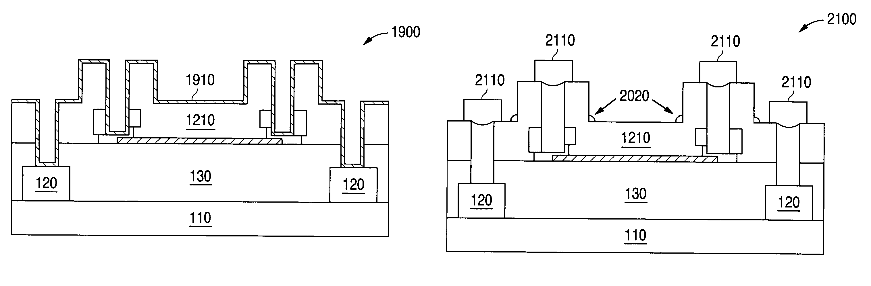
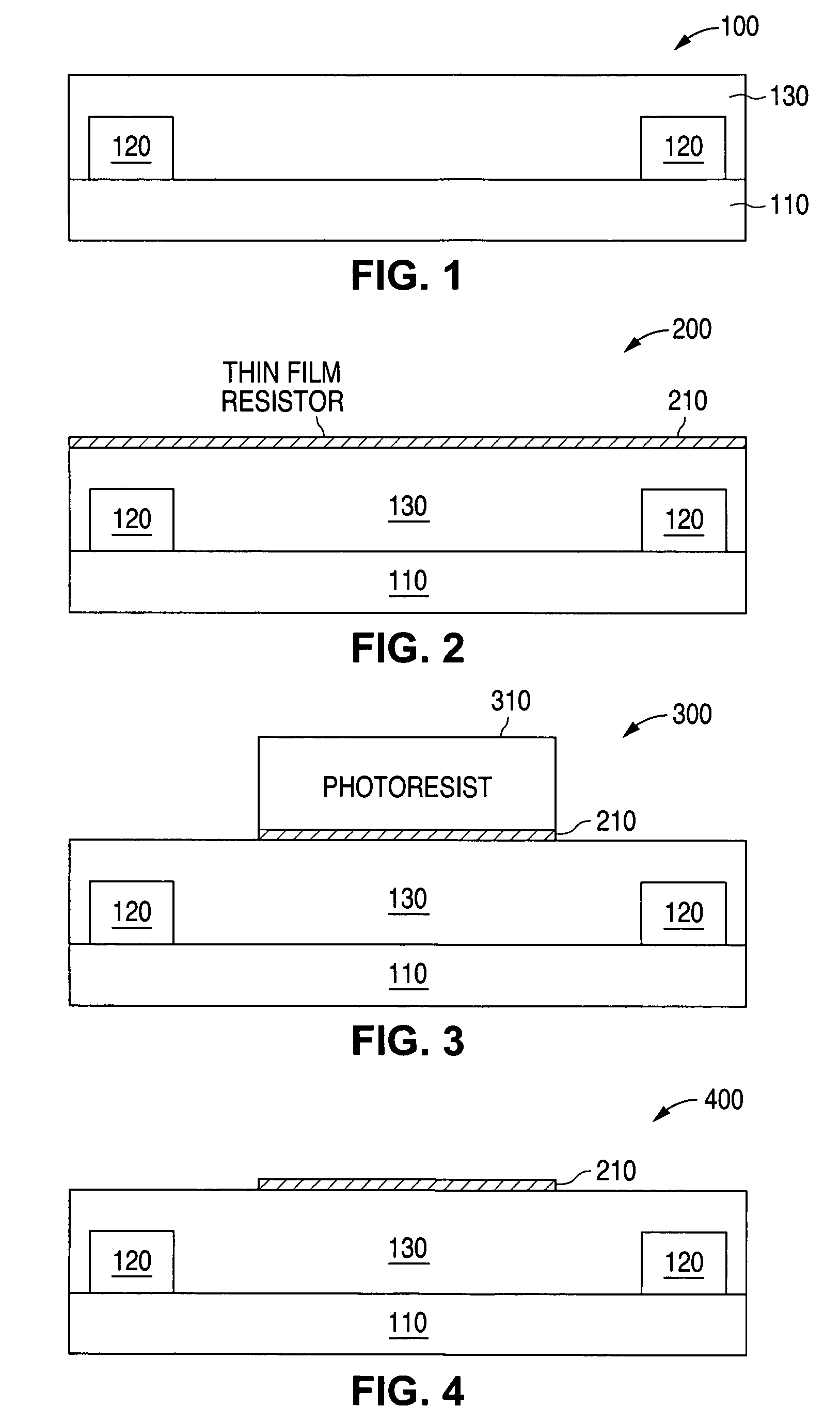
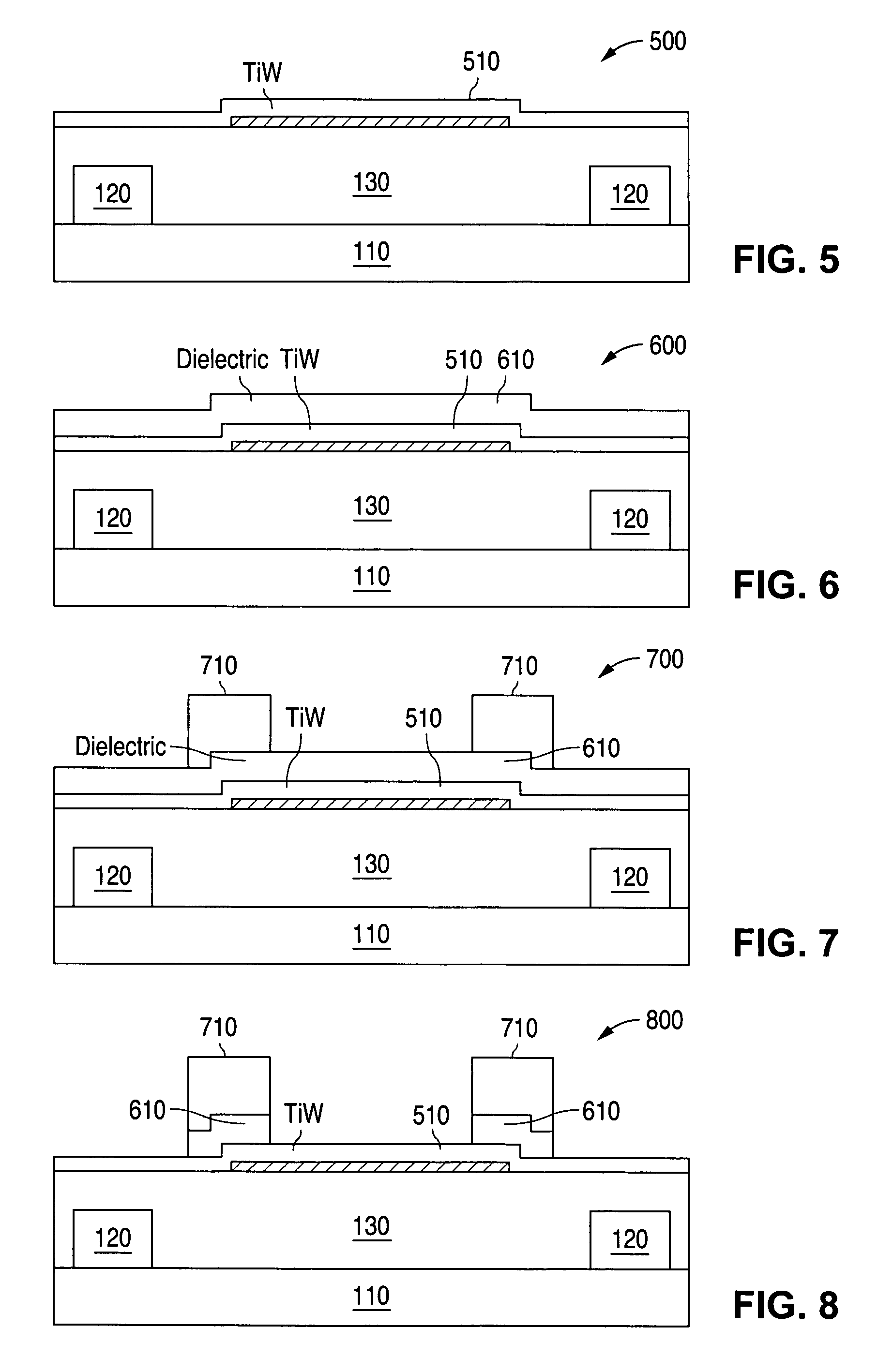
[0049]FIGS. 1 through 23, discussed below, and the various embodiments used to describe the principles of the present invention in this patent document are by way of illustration only and should not be construed in any way to limit the scope of the invention. Persons who are skilled in the art will understand that the principles of the present invention may be implemented in any type of suitably arranged semiconductor device.

[0050]FIG. 1 illustrates a substrate 100 for use in manufacturing a semiconductor device according to the principles of the present invention. The foundation of substrate 100 comprises a first substrate oxide layer 110 on which a patterned first conductor layer 120 is formed. Substrate 100 further comprises a second substrate oxide layer 130 that covers the first substrate oxide layer 110 and the first conductor layer 120. In an advantageous embodiment of the invention the upper surface of the second substrate oxide layer 130 is substantially flat. The upper sur...


PUM


Abstract

A buried thin film resistor having end caps defined by a dielectric mask is disclosed. A thin film resistor is formed on an integrated circuit substrate. A resistor protect layer is formed over the thin film resistor. First and second portions of a first dielectric material are formed over the resistor protect layer over the first and second ends of the thin film resistor. The resistor protect layer is then wet etched using the first and second portions of the first dielectric material as a hard mask. Then a second dielectric layer is deposited. A first via mask and etch process is used to etch vias down to the underlying portions of the resistor protect layer over the ends of the thin film resistor. A second via mask and etch process is used to etch substrate vias to an underlying conductor layer.

Description

RELATED APPLICATIONS[0001]The present application is a continuation-in-part of and claims priority to non-provisional U.S. patent application Ser. No. 11 / 179,022 filed on Jul. 11, 2005 now U.S. Pat. No. 7,332,403.TECHNICAL FIELD OF THE INVENTION[0002]The present invention is generally directed to semiconductor technology and, in particular, to thin film resistors and methods for manufacturing thin film resistors.BACKGROUND OF THE INVENTION[0003]In recent years, there have been great advancements in the speed, power, and complexity of integrated circuits. Some types of integrated circuits comprise thin film resistors. When integrated circuit devices that contain thin film resistors are manufactured, different methods may be employed for manufacturing the thin film resistors.[0004]In some prior art methods for manufacturing a thin film resistor the thin film resistor is located at the same level as a conductor interconnect layer. A major disadvantage of this design is that a resistor ...

Claims


Application Information

Patent Timeline
Patent Type & Authority Patents(United States)
IPC IPC(8): H01L21/20
CPCH01L28/20H01L28/24
Inventor HILL, RODNEYTORRES, VICTORBURGER, MICHAELLINES, TERRY L.
Owner NAT SEMICON CORP
Why Eureka
Try Eureka