Surface acoustic wave device

a surface acoustic wave and waveguide technology, applied in piezoelectric/electrostrictive/magnetostrictive devices, piezoelectric/electrostriction/magnetostriction machines, electrical equipment, etc., can solve problems such as electrostatic discharge damage, damage to electrode digits, and degrade electric characteristics, and achieve the effect of improving the electric characteristic of the saw devi

Active Publication Date: 2008-08-12
SNAPTRACK
View PDF6 Cites 10 Cited by
  • Summary
  • Abstract
  • Description
  • Claims
  • Application Information

AI Technical Summary

Benefits of technology

[0006]To overcome such problems caused by the pyroelectric property, a trace of additive such as iron (Fe) may be added to a piezo-electric substrate. The addition of the additive reduces the volume resistivity of the piezo-electric substrate, prevents a charge from accumulating, and improves the pyroelectric property.
[0008]It is therefore an object of the present invention to provide a more appropriate cut angle for a SAW device which employs an piezo-electric substrate that contains an additive, to further improve the electric characteristic of the SAW device.
[0013]Since a piezo-electric substrate generally has a pyroelectric property as well as a piezo-electric property, a non-uniform charge distribution can appear on the surface of the piezo-electric substrate due to changes in temperature. As such, there is a concern that this charge, if accumulating on the substrate, would give rise to degraded characteristics during manufacturing of the SAW device and during actual use after the SAW device has been mounted on a variety of electronic equipment, and to damages to electrodes due to a discharge in the interdigital transducer. In contrast, if an additive such as Fe is added to a piezo-electric substrate as mentioned above, the volume resistance of the substrate is reduced, thus making it possible to manufacture a SAW device which avoids the foregoing problems and excels in reliability. Moreover, when the cut angle of the substrate is set within the aforementioned range in accordance with the present invention, the resulting SAW device will excel in the electric characteristics.
[0014]While the addition of an additive as mentioned above can improve the pyroelectric property, the present invention does not limit the purpose of adding the additive only to the improvement of the pyroelectric property. In other words, even if an additive is added to a substrate for other purposes than the improvement of the pyroelectric property, the substrate which contains the additive as a result should fall under the piezo-electric substrate as defined in the present invention. This is because even such a substrate is the same in that it contains the additive, and if the substrate is cut at the aforementioned cut angle proposed by the present invention, the substrate likewise provides favorable electric characteristics intended by the present invention.
[0017]According to the present invention, a more appropriate substrate cut angle can be proposed for a SAW device which is manufactured using a piezo-electric substrate to which an additive has been added, so that the resulting SAW device can exhibit favorable electric characteristics (a high Q, a low insertion loss, and the like).

Problems solved by technology

The pyroelectric property can cause a non-uniform charge distribution on the surface of the substrate, associated with changes in temperature, to degrade the electric characteristics of a device, or cause a discharge between the electrodes of a miniature interdigital transducer (IDT) due to an accumulated charge, to damage electrode digits and possibly lead to an electrostatic discharge damage.

Method used


Image

  • Surface acoustic wave device
  • Surface acoustic wave device
  • Surface acoustic wave device

Examples


Embodiment Construction

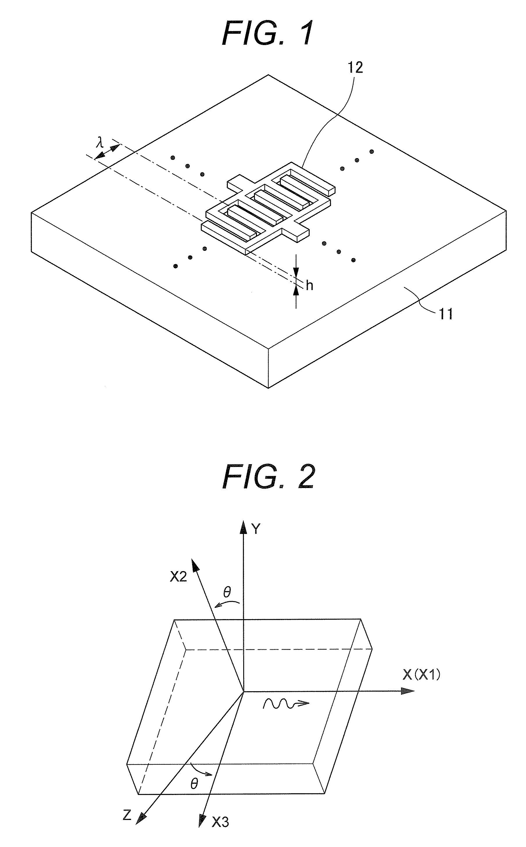
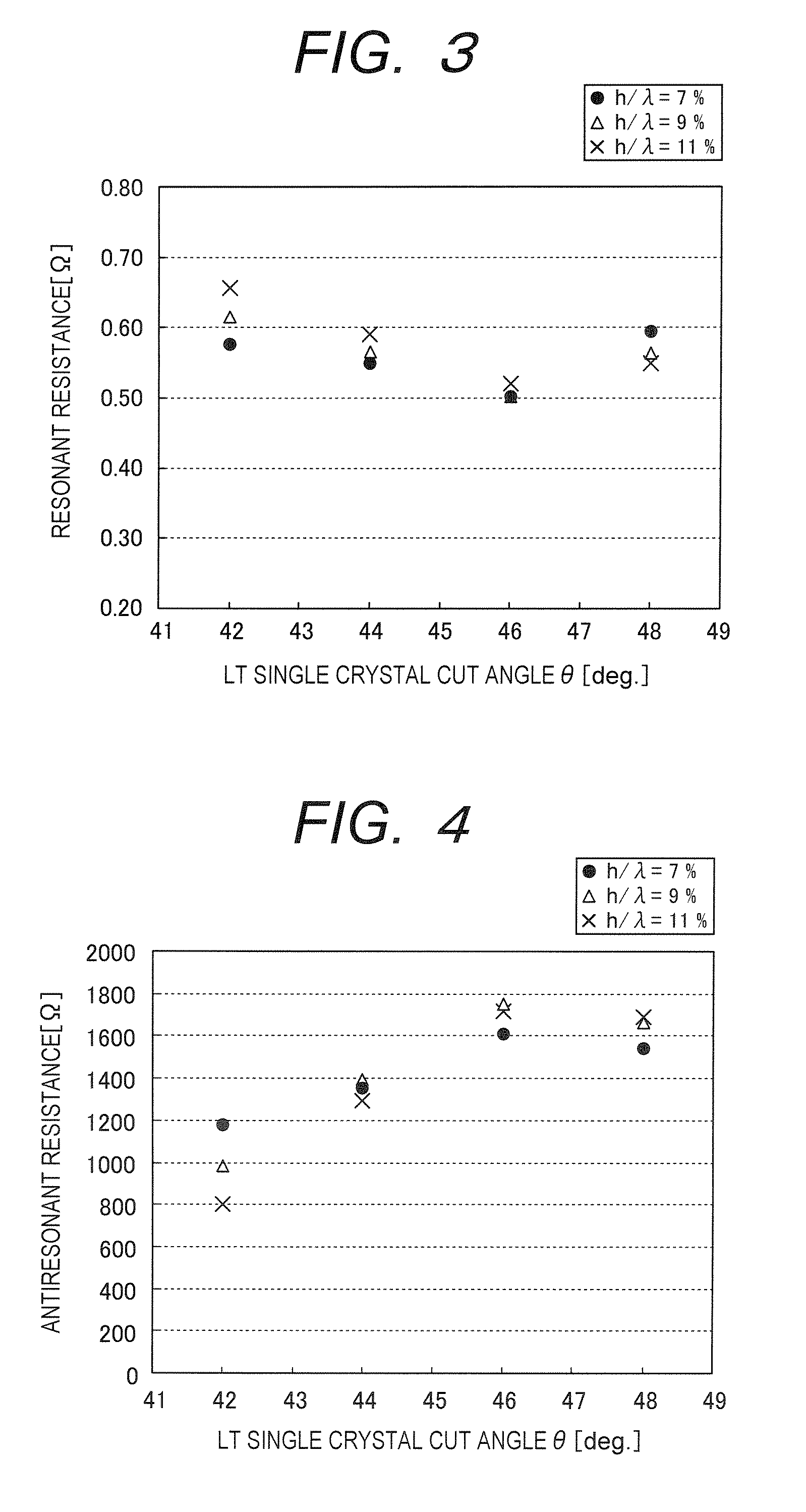
[0024]FIG. 1 is a schematic diagram illustrating a SAW device according to one embodiment of the present invention. As illustrated in FIG. 1, the SAW device comprises an interdigital transducer (made up of interdigital electrodes) 12 formed on the surface of a LT (LiTaO3) single crystal substrate 11. A trace of additive, i.e., Fe by way of example, is added to the LT substrate 11. For adding Fe to the LT substrate 11, Fe may be added to a melted LT material in course of producing a single crystal which forms a substrate (wafer), for example, in the Czochralski process.

[0025]The added Fe causes a reduction in the volume resistivity of the LT substrate 11. In this event, the amount of added Fe is preferably adjusted such that the volume resistivity of the LT substrate 11 falls within a range of 3.6×10¹⁰ to 1.5×10¹⁴Ω·cm. This is because the volume resistivity equal to or lower than 1.5×10¹⁴Ω·cm will prevent a charge from accumulating on the LT substrate 11 to avoid damages to the inter...


PUM

PropertyMeasurementUnit
volume resistivityaaaaaaaaaa
anglesaaaaaaaaaa

Abstract

A SAW device comprises a single crystal piezo-electric strate (made, for example, of LiTaO3 or LiNbO3), and an interdigital transducer (IDT) formed of a material mainly containing Al and disposed on the piezo-electric substrate. The piezo-electric strate contains an additive (for example, Fe, Mn, Cu, Ti), and an orientation rotated by an angle in a range of 42° to 48° (more preferably 46°±0.3°) from a Y-axis toward a Z-axis about an X-axis. The IDT presents a normalized thickness h / λ (h: thickness of electrode, and λ: spacing between digits of the IDT) of 7% to 11%. A more appropriate substrate cut angle can be shown for the SAW device which employs a piezo-electric substrate containing an additive, to improve the electric characteristics thereof.

Description

BACKGROUND OF THE INVENTION[0001]The present invention relates to a surface acoustic wave device, and more particularly, to a substrate cut angle which is suitable for a single crystal piezo-electric substrate to which an additive is added to constitute a surface acoustic wave device.[0002]A surface acoustic wave device (hereinafter called the “SAW device”) which utilizes a surface acoustic wave (SAW) generated by a piezo-electric effect is widely applied to portable telephones and other electronic equipment as an electronic device such as a filter, a resonator and the like, because of its small size and light weight as well as high reliability.[0003]The SAW device generally comprises a first electrode which is applied with a high frequency signal to excite a surface acoustic wave, a second electrode which receives the surface acoustic wave propagated thereto after excited by the first electrode, and converts the surface acoustic wave again to an electric signal to extract a signal ...

Claims


Application Information

Patent Timeline
Patent Type & Authority Patents(United States)
IPC IPC(8): H03H9/145H01L41/047H03H9/25
CPCH03H9/02921H03H9/02559
Inventor KIHARA, YOSHIKAZUOSANAI, KATSUNORIHIROKAWA, YUKIOSOBU, MASAKI
Owner SNAPTRACK
Why Eureka
Try Eureka