Dual-band voltage-controlled oscillator using bias switching and output-buffer multiplexing

a voltage control and output buffer technology, applied in the direction of pulse generators, pulse techniques, electric pulse generator circuits, etc., can solve the problems of large overall area, poor phase noise characteristics, and difficulty in implementing resonant characteristics of lc tanks, so as to reduce interference and enhance phase noise characteristics

Active Publication Date: 2008-08-19
SAMSUNG ELECTRONICS CO LTD
View PDF7 Cites 7 Cited by
  • Summary
  • Abstract
  • Description
  • Claims
  • Application Information

AI Technical Summary

Benefits of technology

[0011]The present invention has been developed in order to solve the above drawbacks and other problems associated with the conventional arrangement. An aspect of the present invention is to provide a dual-band oscillator integrated in high density into one chip through a CMOS process, and using bias switching and output-buffer multiplexing to reduce interference between the dual-band oscillators, thereby enhancing phase noise characteristics.

Problems solved by technology

Such a dual-band voltage-controlled oscillator has a problem in that an output signal at the common source terminal (node A) has a small magnitude and poor phase noise characteristics due to interference between frequencies.
The above structure has a problem that its overall area is increased since additional circuits such as mixers and notch filters are required.
Such a method has difficulty in implementing resonant characteristics of the LC tank since values of the inductors and capacitors need to change in a wide range and MOS switches are added in order to obtain a frequency two times higher than an oscillation frequency.
Further, the method has a problem of increased chip area due to the addition of inductors and capacitors.

Method used


Image

  • Dual-band voltage-controlled oscillator using bias switching and output-buffer multiplexing
  • Dual-band voltage-controlled oscillator using bias switching and output-buffer multiplexing
  • Dual-band voltage-controlled oscillator using bias switching and output-buffer multiplexing

Examples


Embodiment Construction

[0026]Hereinafter, the present invention will be described with reference to the accompanying drawings.

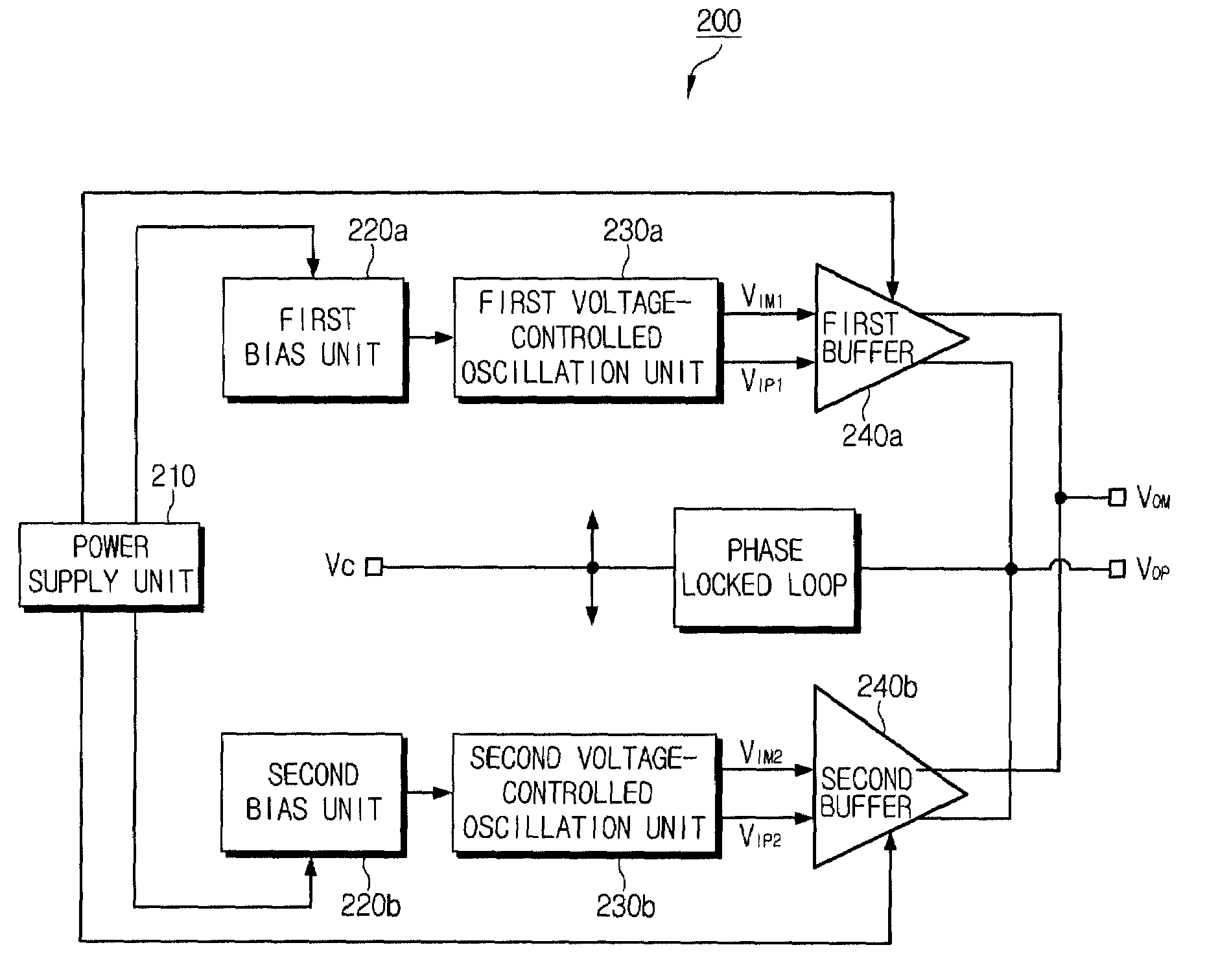
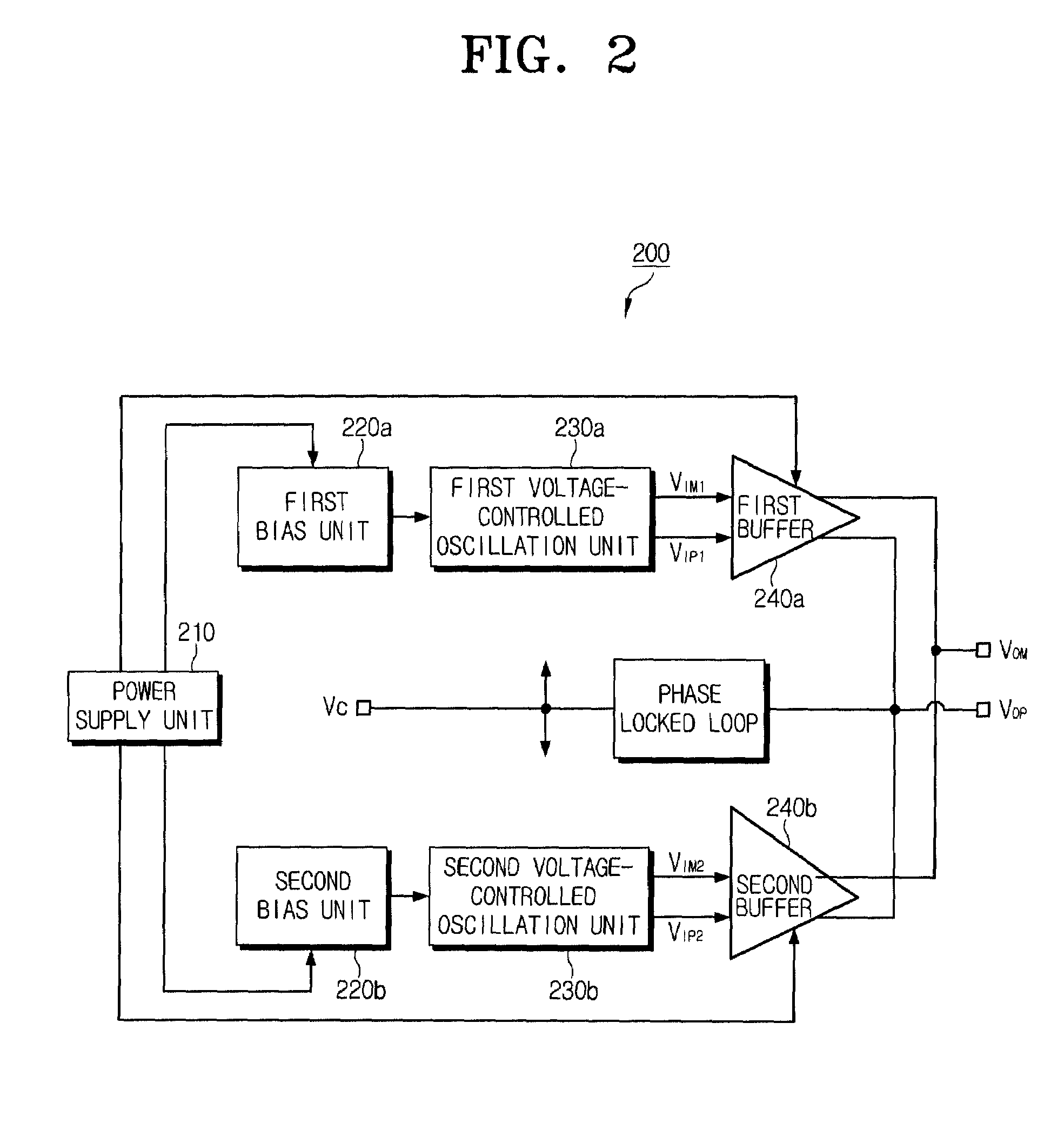
[0027]FIG. 2 is a view for showing a structure of a dual-band voltage-controlled oscillator using bias switching and output-buffer multiplexing according to an embodiment of the present invention. In FIG. 2, the dual-band voltage-controlled oscillator 200 has a power supply unit 210, plural bias units including a first bias unit 220a and a second bias unit 220b, plural voltage-controlled oscillation units including a first voltage-controlled oscillation unit 230a and a second voltage-controlled oscillation unit 230b, and plural buffers including a first buffer 240a and a second buffer 240b.

[0028]The power supply unit 210 supplies a voltage of predetermined level to and drives the first and second bias units 220a and 220b and the first and second buffers 240a and 240b.

[0029]The plural bias units consist of the first bias unit 220a and the second bias unit 220b. If the power supply...


PUM


Abstract

Disclosed is a dual-band voltage-controlled oscillator using bias switching and output-buffer multiplexing. The dual-band voltage-controlled oscillator includes a power supply unit for supplying a source voltage; plural voltage-controlled oscillation units for outputting different oscillation frequencies according to controls of a certain tuning voltage; plural bias units for generating driving voltages for driving the voltage-controlled oscillation units and supplying the driving voltages to the voltage-controlled oscillation units; and plural buffers for selectively outputting oscillation frequencies of the plural voltage-controlled oscillation units. The present invention implements the dual-band voltage-controlled oscillator through bias switching and output-buffer multiplexing, which brings an advantage of elimination of interference between output frequencies to enhance phase noise characteristics.

Description

CROSS-REFERENCE TO RELATED APPLICATIONS[0001]This application claims benefit under 35 U.S.C. § 119 from Korean Patent Application No. 2005-08613, filed on Jan. 31, 2005, the entire contents of which are incorporated herein by reference.BACKGROUND OF THE INVENTION[0002]1. Field of the Invention[0003]The present invention relates to a dual-band voltage-controlled oscillator, and more particularly to a dual-band voltage-controlled oscillator having less interference between oscillators and improved phase-noise characteristics by using bias switching and output-buffer multiplexing.[0004]2. Description of the Related Art[0005]As wireless communication services advance, next-generation wireless communication services such as wireless local loop (WLL) and International Mobile Telecommunications 2000 (IMT-2000) will be launched in the future together with the digital mobile phones and personal communication services (PCSs) in commercial services. The next-generation wireless communication s...

Claims


Application Information

Patent Timeline
Patent Type & Authority Patents(United States)
IPC IPC(8): H03B5/12
CPCH03B5/1228H03B5/124H03B5/1209H03B5/1215A01G31/02Y02P60/21
Inventor JEON, SANG-YOONLEE, HEUNG-BAELEE, SEONG-SOOLIM, JINUPCHOI, JOONGHO
Owner SAMSUNG ELECTRONICS CO LTD
Why Eureka
Try Eureka