Pixel current driver for organic light emitting diode displays

a technology of light-emitting diodes and current drivers, which is applied in the direction of static indicating devices, identification means, instruments, etc., can solve the problems of not supporting the resolution needed in the next-generation display, electrodes can give rise to parasitic capacitance, and the effect of significant effects is not realized, so as to minimize the charge induced in the top channel of the tft, enhance the circuit performance, and minimize the leakage current in the tft

Inactive Publication Date: 2008-08-19
IGNIS INNOVATION
View PDF33 Cites 250 Cited by
  • Summary
  • Abstract
  • Description
  • Claims
  • Application Information

AI Technical Summary

Benefits of technology

[0007]Accordingly, it is an object of the present invention to provide to a pixel current driver for an organic light emitting display(OLED), capable of minimizing parasitic couplings between the OLED and the transistor layers.
[0008]In order to achieve the above object, a pixel current driver for OLED layer for emitting light according to the present invention comprises a plurality of thin film transistors (TFTs) each having dual gates and for driving the OLED layer. A top gate of the dual gates is formed between a source and a drain of each of the thin film transistors, to thereby minimize parasitic capacitance.
[0012]With the above structure of an a-Si:H current driver according to the present invention, the charge induced in the top channel of the TFT is minimized, and the leakage currents in the TFT is minimized so as to enhance circuit performance.

Problems solved by technology

Despite the OLED's demonstrated superiority over the LCD, there still remain several challenging issues related to encapsulation and lifetime, yield, color efficiency, and drive electronics, all of which are receiving considerable attention.
Although passive matrix addressed OLED displays are already in the marketplace, they do not support the resolution needed in the next generation displays, since high information content (HIC) formats are only possible with the active matrix addressing scheme.
However, this continuous back electrode can give rise to parasitic capacitance, whose effects become significant when the electrode runs over the switching and other thin film transistors (TFTs).
Here, the presence of the back electrode can induce a parasitic channel in TFTs giving rise to high leakage current.

Method used


Image

  • Pixel current driver for organic light emitting diode displays
  • Pixel current driver for organic light emitting diode displays
  • Pixel current driver for organic light emitting diode displays

Examples


Embodiment Construction

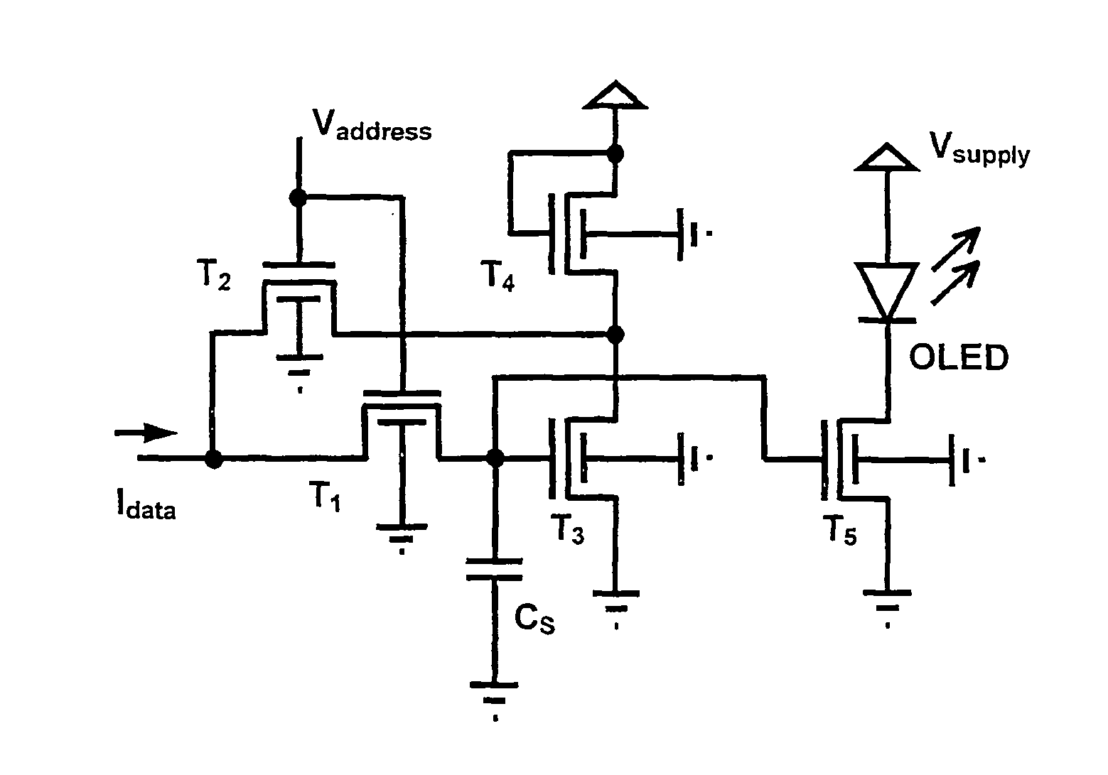
[0031]Although amorphous Si does not enjoy equivalent electronic properties compared to poly-Si, it adequately meets many of the drive requirements for small area displays such as those needed in pagers, cell phones, and other mobile devices. Poly-Si TFTs have one key advantage in that they are able to provide better pixel drive capability because of their higher mobility, which can be of the order of μFE˜100 cm2 / Vs. This makes poly-Si highly desirable for large area (e.g. laptop size) VGA and SVGA displays. The lower mobility associated with a-Si:H TFTs (μFE˜1 cm2 / Vs) is not a limiting factor since the drive transistor in the pixel can be scaled up in area to provide the needed drive current. The OLED drive current density is typically 10 mA / cm2 at 10V operation to provide a brightness of 100 cd / m2—the required luminance for most displays. For example, with an a-Si:H TFT mobility of 0.5 cm2 / Vs and channel length of 25 μm, this drive current requirement translates into required pixe...


PUM


Abstract

A pixel current driver comprises a plurality of thin film transistors (TFTs) each having dual gates and for driving OLED layers. A top gate of the dual gates is formed between a source and a drain of each of the thin film transistors, to thereby minimize parasitic capacitance. The top gate is grounded or electrically tied to a bottom gate. The plurality of thin film transistors may be two thin film transistors formed in voltage-programmed manner or five thin film transistors formed in a current-programmed ΔVT-compensated manner. Other versions of the current-programmed circuit with different numbers of thin film transistors are also presented that compensate for δVT. The OLED layer are continuous and vertically stacked on the plurality of thin film transistors to provide an aperture ratio close to 100%.

Description

[0001]This application is a continuation application of U.S. patent application Ser. No. 10 / 468,319 filed Jan. 23, 2004 now abandoned, which is the U.S. National Phase of PCT / CA02 / 00173 having an International Filing Date of Feb. 18, 2002, which claims the benefit of U.S. Provisional Patent Application Ser. No. 60 / 268,900 filed on Feb. 16, 2001.BACKGROUND OF THE INVENTION[0002]1. Field of the Invention[0003]The present invention relates to a an organic light emitting diode display, and more particularly to an a pixel current driver for an organic light emitting display (OLED), capable of minimizing parasitic couplings between the OLED and the transistor layers.[0004]2. Description of the Prior Art[0005]OLED displays have gained significant interest recently in display applications in view of their faster response times, larger viewing angles, higher contrast, lighter weight, lower power, amenability to flexible substrates, as compared to liquid crystal displays (LCDs). Despite the O...

Claims


Application Information

Patent Timeline
Patent Type & Authority Patents(United States)
IPC IPC(8): G09G3/32H01L51/50G09F9/30G09G3/20G09G3/30H01L21/336H01L27/12H01L27/15H01L27/32H01L29/786
CPCG09G3/3233G09G3/3241H01L27/3276G09G2300/0804H01L27/12H01L27/283G09G2320/0223H10K19/10H10K59/131
Inventor NATHAN, AROKIASERVATI, PEYMANSAKARIYA, KAPILKUMAR, ANIL
Owner IGNIS INNOVATION
Why Eureka
Try Eureka