Methods of forming self-aligned contact structures in semiconductor integrated circuit devices

a technology of integrated circuit devices and contact structures, which is applied in the direction of semiconductor devices, electrical devices, transistors, etc., can solve the problems of exposing patterns in an adverse manner, and achieve the effect of improving the reliability of alignment techniques and minimizing parasitic capacitan

Inactive Publication Date: 2005-04-19
SAMSUNG ELECTRONICS CO LTD
View PDF22 Cites 28 Cited by
  • Summary
  • Abstract
  • Description
  • Claims
  • Application Information

AI Technical Summary

Benefits of technology

[0007]It is therefore an object of the present invention to provide methods of forming self-aligned contact structure, which can minimize the parasitic capacitance between two adjacent conductive layers and improve the reliability of the alignment techniques.

Problems solved by technology

These methods improve process reliability by reducing the likelihood that contact holes will become misaligned to underlying integrated circuit device patterns and thereby potentially expose the patterns in an adverse manner.

Method used


Image

  • Methods of forming self-aligned contact structures in semiconductor integrated circuit devices
  • Methods of forming self-aligned contact structures in semiconductor integrated circuit devices
  • Methods of forming self-aligned contact structures in semiconductor integrated circuit devices

Examples


Embodiment Construction

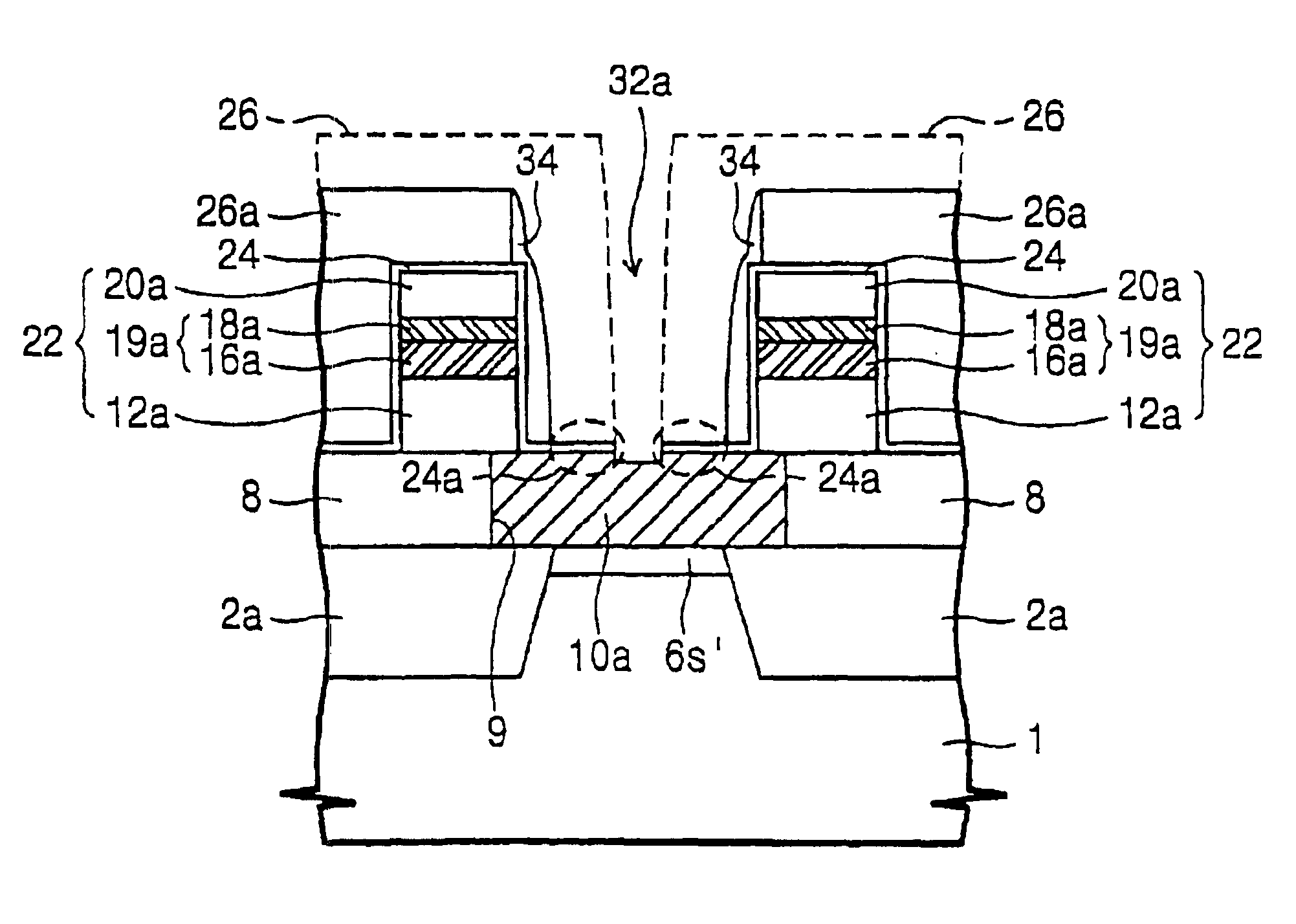
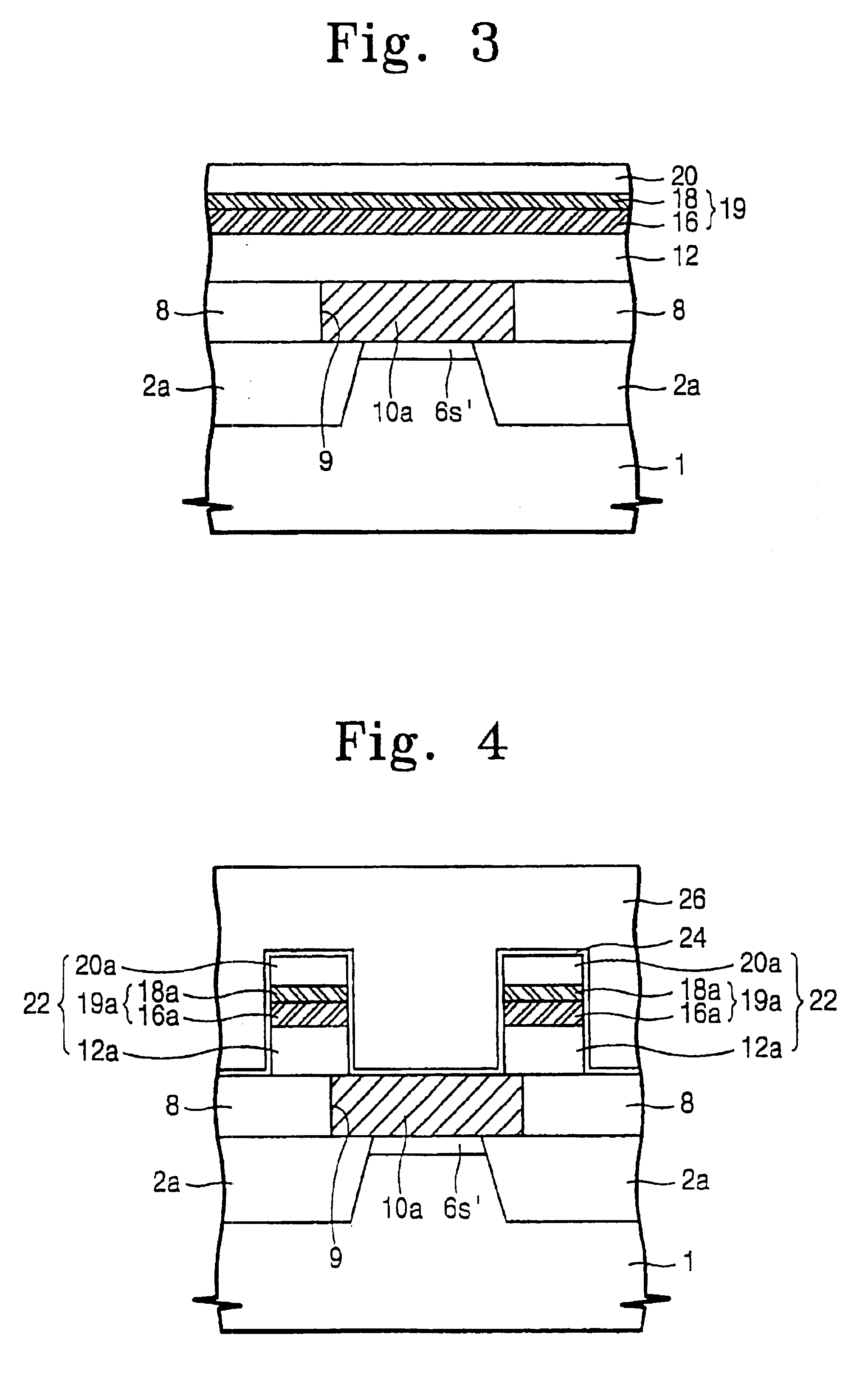
[0014]The present invention will now be described more fully hereinafter with reference to the accompanying drawings, in which preferred embodiments of the invention are shown. This invention may, however, be embodied in different forms and should not be construed as limited to the embodiments set forth herein. Rather, these embodiments are provided so that this disclosure will be thorough and complete, and will fully convey the scope of the invention to those skilled in the art. In the drawings, the thickness of layers and regions are exaggerated for clarity. It will also be understood that when a layer is referred to as being “on” another layer or substrate, it can be directly on the other layer or substrate, or intervening layers may also be present. Like numbers refer to like elements throughout.

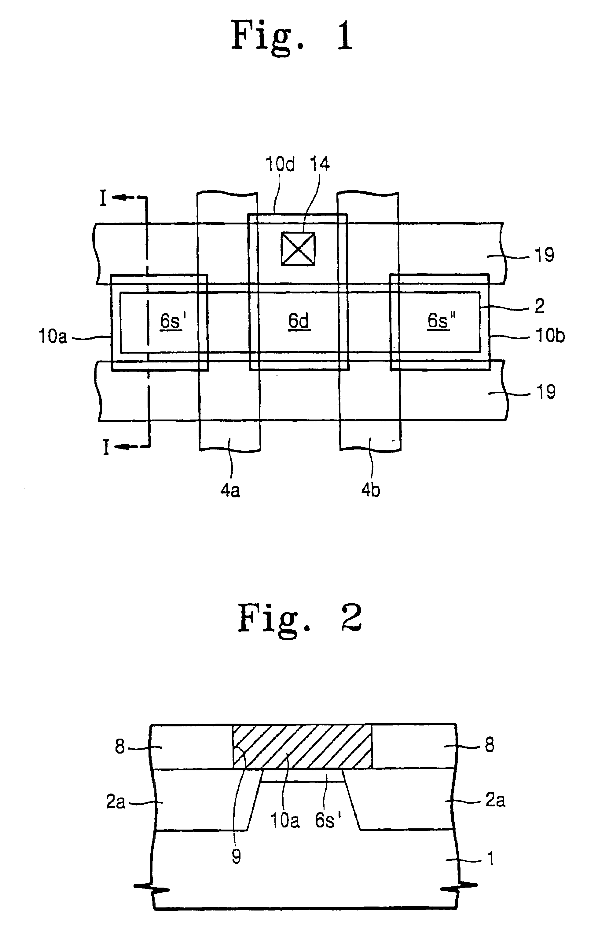
[0015]FIG. 1 is a top plan view of a portion of a typical DRAM cell array region.

[0016]Referring to FIG. 1, an active region 2 is defined at a predetermined region of a P-type semiconduc...


PUM


Abstract

Methods of forming integrated circuit devices (e.g., memory devices) include the use of preferred self-aligned contact hole fabrication steps. These steps improve process reliability by reducing the likelihood that contact holes will become misaligned to underlying integrated circuit device structures and thereby potentially expose the structures in an adverse manner. Typical methods include the steps of forming a plurality of interconnection patterns on a substrate and then covering a surface of the interconnection patterns and a portion of the substrate with a capping insulating layer such as silicon nitride layer. The capping insulating layer is then covered with an upper interlayer insulating layer different from the capping insulating layer. The upper interlayer insulating layer and the capping insulating layer are then dry-etched in sequence to form a first narrow contact hole that exposes the substrate, but preferably does not expose the interconnection patterns. The first contact hole is then widened in a self-aligned manner using the capping insulating layer as an etch-stop layer. This widening step is performed by wet etching sidewalls of the first contact hole using an etchant that etches the upper interlayer insulating layer faster than the capping insulating layer. In this manner, the first contact hole may be formed to initially compensate for potential misalignment errors and then a self-aligned wet etching step may be performed to widen the first contact hole into a second contact hole so that low resistance contacts (e.g., contact plugs) can be provided therein.

Description

RELATED APPLICATIONS[0001]This application is a divisional of U.S. application Ser. No. 09 / 556,499, filed Apr. 24, 2000 now U.S. Pat. No. 6,649,508, which is related to Korean Application No. 2000-5358, filed Feb. 3, 2000, the disclosures of which are hereby incorporated herein by reference.FIELD OF THE INVENTION[0002]This invention relates to integrated circuit device fabrication methods and, more particularly, to methods of forming self-aligned contact structures in semiconductor integrated circuit devices.BACKGROUND OF THE INVENTION[0003]Attempts to increase device integration density in microelectronic integrated circuits have typically resulted in the fabrication of smaller and smaller devices that are spaced more closely together. In order to electrically access these devices, conventional techniques to photolithographically define the location of contact holes to these devices have also had to improve. Such improvements have typically included the development of photolithogra...

Claims


Application Information

Patent Timeline
Patent Type & Authority Patents(United States)
IPC IPC(8): H01L21/60H01L21/70H01L21/8242H01L21/02H01L21/28H01L21/768H01L21/82H01L27/108
CPCH01L21/76897H01L27/10855H01L27/10885H01L21/76831H10B12/0335H10B12/482H01L21/82
Inventor PARK, JONG-WOOKIM, YUN-GIPARK, DONG-GUN
Owner SAMSUNG ELECTRONICS CO LTD
Why Eureka
Try Eureka