Method of forming a trench isolation layer and method of manufacturing a non-volatile memory device using the same

Inactive Publication Date: 2006-05-04
SAMSUNG ELECTRONICS CO LTD
View PDF3 Cites 28 Cited by
  • Summary
  • Abstract
  • Description
  • Claims
  • Application Information

AI Technical Summary

Benefits of technology

[0012] Accordingly, the present invention provides a method of fo

Problems solved by technology

However, recent high integration degree in a non-volatile memory device has remarkably reduced a cell distance between cells adjacent to each other in the non-volatile memory device, so that parasitic capacitance between the floating gates in the neighboring cells is no longer negligible.
Particularly, the above threshold voltage variation causes an operation failure, for example, a r

Method used


Image

  • Method of forming a trench isolation layer and method of manufacturing a non-volatile memory device using the same
  • Method of forming a trench isolation layer and method of manufacturing a non-volatile memory device using the same
  • Method of forming a trench isolation layer and method of manufacturing a non-volatile memory device using the same

Examples


embodiment 1

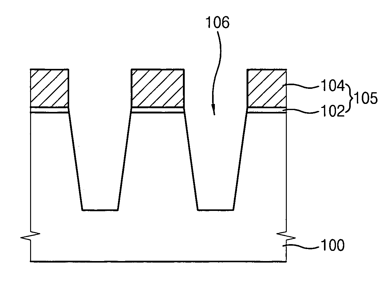
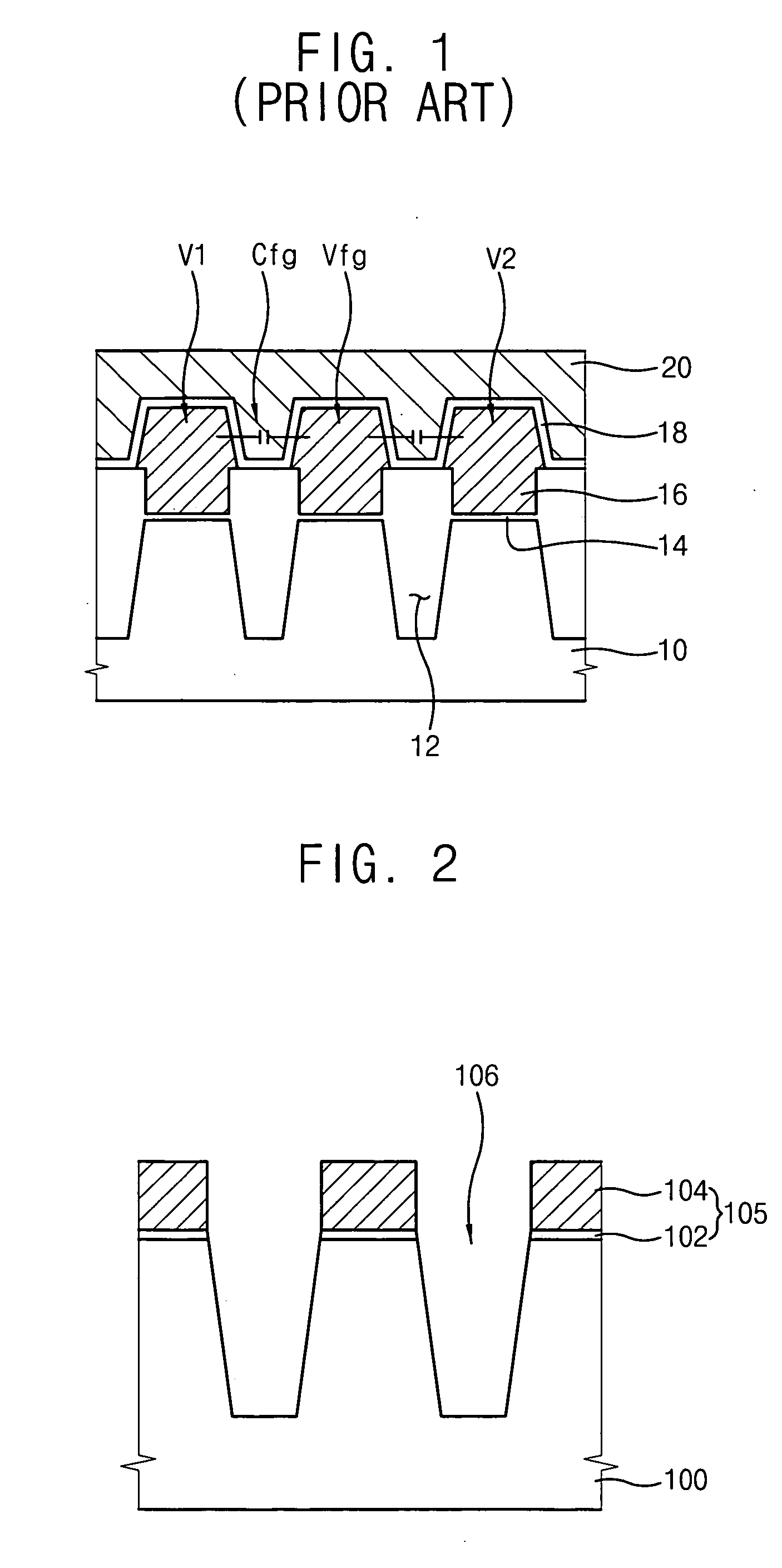
[0031] FIGS. 2 to 6 are cross-sectional views illustrating processing steps for a method of forming a device isolation layer according to a first exemplary embodiment of the present invention.

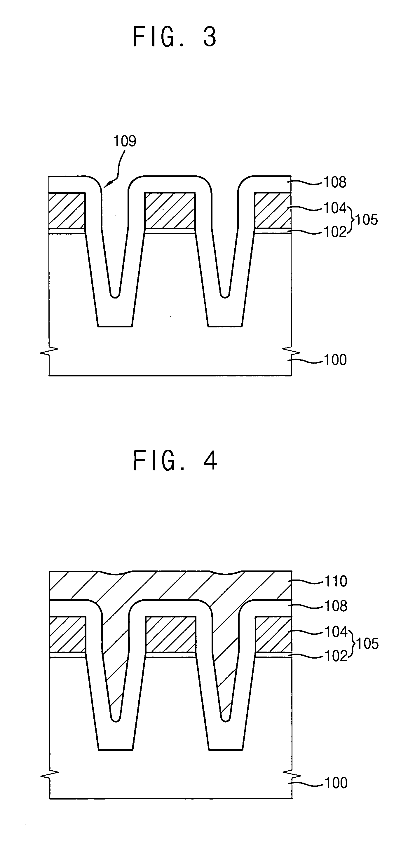
[0032] Referring to FIG. 2, a pad oxide layer (not shown) is formed on a substrate 100 to a thickness of about 50 Å to about 200 Å for reducing stress when silicon nitride is deposited in a subsequent process. A silicon nitride layer (not shown) is formed on the pad oxide layer. Then, the silicon nitride layer and the pad oxide layer are partially and sequentially etched away, thereby forming a pad oxide pattern 102 and a silicon nitride pattern 104 sequentially stacked on the substrate 100. In the present embodiment, the pad oxide pattern 102 and the silicon nitride pattern 104 function as a hard mask pattern 105 in a subsequent process. The surface portion of the substrate 100 is etched away using the hard mask pattern 105 as an etching mask, thereby forming a trench 106 by which conductive ...

embodiment 2

[0051] FIGS. 7 to 12 are cross-sectional views illustrating processing steps for a method of manufacturing a semiconductor device according to a second exemplary embodiment of the present invention. A device isolation layer for the semiconductor device is formed in the same or similar way as in Embodiment 1, described above.

[0052] Referring to FIG. 7, the same process as described with reference to FIGS. 2 to 4 is performed on a semiconductor substrate 150. As described above, a pad oxide layer (not shown) and a silicon nitride layer (not shown) are formed on the substrate 150 for reducing stress during formation of the silicon nitride layer. The silicon nitride layer functions as a mask layer for forming the device isolation layer, and also defines a floating gate region in which a floating gate is formed in subsequent processes. As a result, the silicon nitride layer is formed to a thickness greater than that of a desired floating gate.

[0053] Then, the silicon nitride layer and ...

embodiment 3

[0084] FIGS. 15 to 19 are cross-sectional views illustrating processing steps for a method of manufacturing a non-volatile memory device according to a third exemplary embodiment of the present invention.

[0085] Referring to FIG. 15, a tunnel oxide layer (not shown) is formed on a substrate 300. Examples of the tunnel oxide layer include a silicon oxide layer, a silicon oxide layer doped with fluorine, a silicon oxide layer doped with carbon, a material layer comprised of a low dielectric material such as low-k material, etc.

[0086] A first polysilicon layer (not shown) is formed on the tunnel oxide layer so as to form a lower floating gate pattern, and a silicon nitride layer (not shown) is formed on the first polysilicon layer so as to form a hard mask layer.

[0087] The silicon nitride layer is patterned through a photolithography process, thereby forming a hard mask pattern 306. The first polysilicon layer and the tunnel oxide layer are sequentially and partially etched away usin...


PUM


Abstract

In a method of forming a device isolation layer for minimizing a parasitic capacitor and a non-volatile memory device using the same, a trench is formed on a substrate. A first insulation layer is formed on a top surface of the substrate and on inner surfaces of the trench, so that the trench is partially filled with the first insulation layer. A second insulation layer is formed on the first insulation layer to a thickness to fill up the trench, thereby forming a preliminary isolation layer. An etching rate of the second insulation layer is different from that of the first insulation layer. A recess is formed at a central portion of the preliminary isolation layer by partially removing the first and second insulation layers, thereby forming the device isolation layer including the recess. The recess in the device isolation layer reduces a parasitic capacitance in a non-volatile memory device.

Description

CROSS-REFERENCE TO RELATED APPLICATION [0001] This application claims priority to Korean Patent Application No. 2004-89213 filed on Nov. 4, 2004, the content of which is herein incorporated by reference in its entirety. FIELD OF THE INVENTION [0002] The present invention relates generally to semiconductor devices and, more particularly, to non-volatile memory devices. BACKGROUND OF INVENTION [0003] Non-volatile memory devices can maintain stored data even after power to the devices is turned off, and have an advantage in that the data stored in the non-volatile memory devices may be electrically erasable or programmable. For those reasons, non-volatile memory devices have been widely used in various portable electronic appliances for storing data. Recently, non-volatile memory devices have been used in highly technical appliances, such as digital cameras, MP3 players, cellular phones, etc. [0004]FIG. 1 is a cross sectional view illustrating a conventional non-volatile memory device....

Claims


Application Information

Patent Timeline
IPC IPC(8): H01L21/76
CPCH01L21/76232H01L27/115H01L27/11521H10B69/00H10B41/30H01L21/76H10B99/00
Inventor CHOI, JONG-WANKIM, HONG-GUNNA, KYU-TAEHONG, EUNKEE
Owner SAMSUNG ELECTRONICS CO LTD
Why Eureka
Try Eureka