Wideband optical coupling into thin SOI CMOS photonic integrated circuit

Active Publication Date: 2008-08-19
CISCO TECH INC
View PDF12 Cites 27 Cited by
  • Summary
  • Abstract
  • Description
  • Claims
  • Application Information

AI Technical Summary

Problems solved by technology

However, this success has been shown only within research / development environments, where there is careful control over fabrication conditions.

Method used


Image

  • Wideband optical coupling into thin SOI CMOS photonic integrated circuit
  • Wideband optical coupling into thin SOI CMOS photonic integrated circuit
  • Wideband optical coupling into thin SOI CMOS photonic integrated circuit

Examples


Embodiment Construction

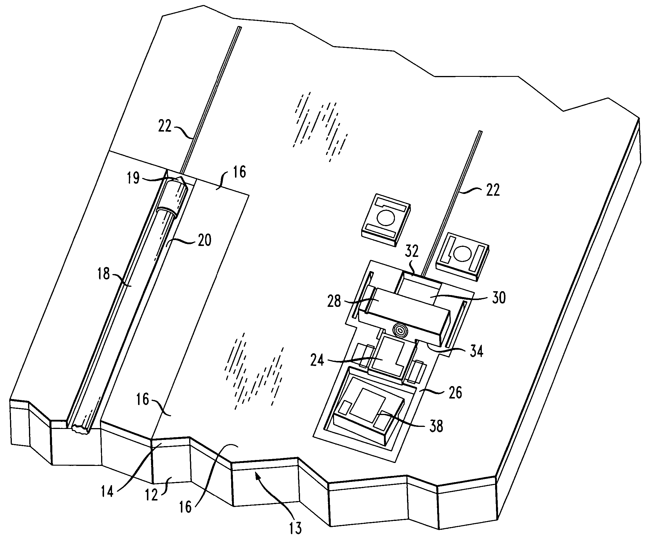
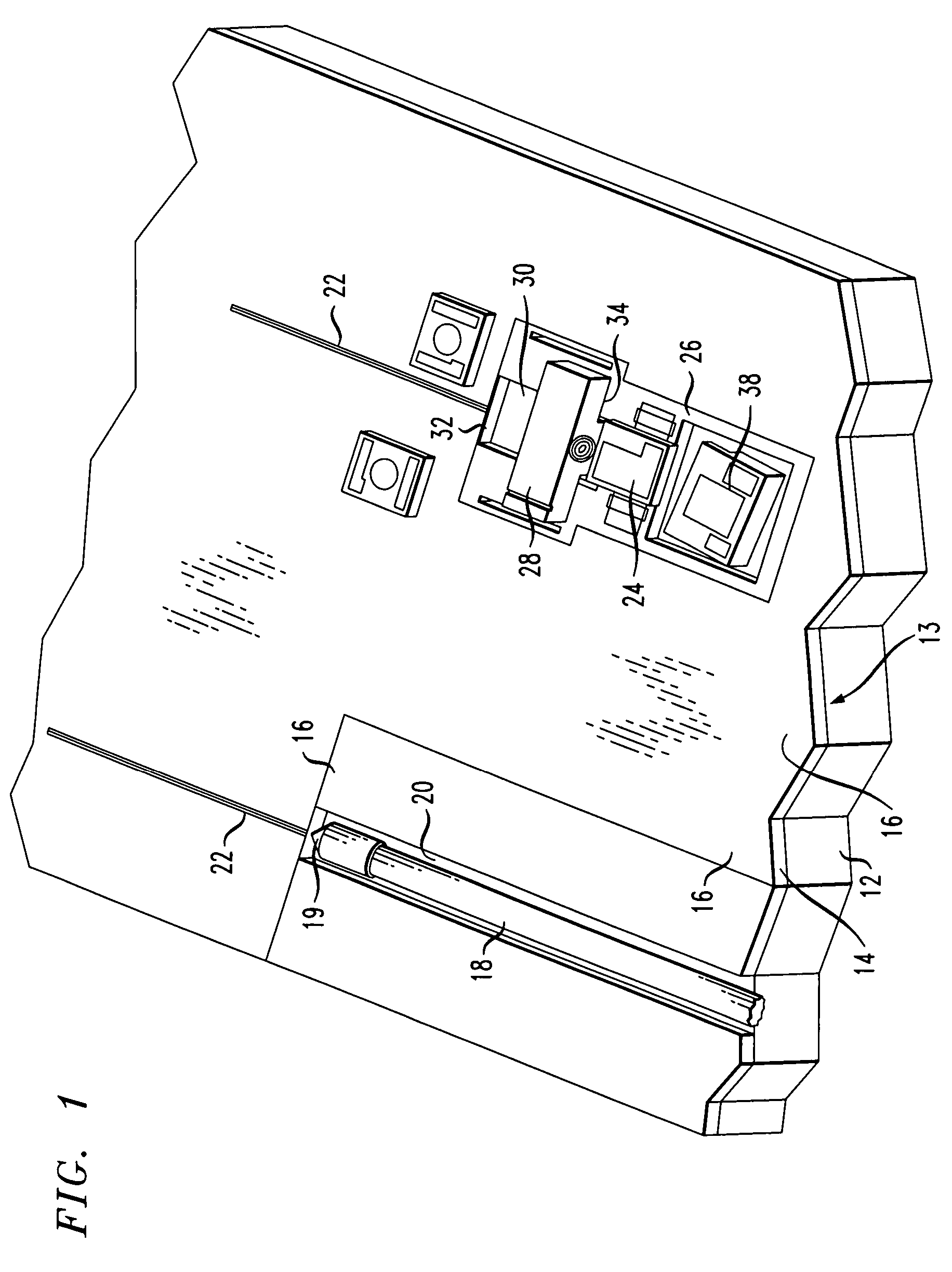
[0022]FIG. 1 is an isometric view of an exemplary SOI structure 10 formed to include both a fiber coupling arrangement and a laser coupling arrangement of the present invention. It is to be understood that any number of fiber-based couplings and / or laser-based couplings may be utilized on a given SOI structure. The pair of couplings is shown here only for the sake of discussion and explanation.

[0023]As shown, SOI structure 10 comprises a silicon substrate 12, a buried oxide (BOX) layer 14 and a sub-micron thick, single crystal silicon surface layer 16 (hereinafter referred to as “SOI layer 16”). It is an important feature of the present invention that by utilizing a sub-micron dimensioned optical waveguide within SOI layer 16, the nanotaper coupling arrangement can be configured to be essentially polarization independent. That is, both the TE and TM optical modes will couple into the waveguide with essentially the same coupling efficiency. One exemplary configuration (for use in ass...


PUM


Abstract

An arrangement for providing optical coupling into and out of a relatively thin silicon waveguide formed in the SOI layer of an SOI structure includes a lensing element and a defined reference surface within the SOI structure for providing optical coupling in an efficient manner. The input to the waveguide may come from an optical fiber or an optical transmitting device (laser). A similar coupling arrangement may be used between a thin silicon waveguide and an output fiber (either single mode fiber or multimode fiber).

Description

CROSS-REFERENCE TO RELATED APPLICATION[0001]This application claims the benefit of U.S. Provisional Application No. 60 / 757,962, filed Jan. 11, 2006.TECHNICAL FIELD[0002]The present invention relates to an apparatus for providing coupling into and out of a thin (i.e., sub-micron dimensioned) optical waveguide and, more particularly, to the use of reference planes and lensing elements to provide coupling between a fiber or lens and a thin waveguide.BACKGROUND OF THE INVENTION[0003]A common prior art technique for coupling light from an external source to a silicon waveguide is to cleave or polish end facets on both the waveguide and the mating fiber termination. Examples of fiber terminations include, but are not limited to: multimode or single-mode fibers with small or zero cleave / polish angles, and specially-shaped or lensed single-mode fibers that produce spot sizes as small as 1.5 μm. The fiber termination is aligned to allow maximum light transmission through the waveguide, and t...

Claims


Application Information

Patent Timeline
Patent Type & Authority Patents(United States)
IPC IPC(8): G02B6/10G02B6/12G02B6/26G02B6/30G02B6/32
CPCG02B6/4231G02B6/12
Inventor GHIRON, MARGARETGOTHOSKAR, PRAKASHFANGMAN, JOHNMONTGOMERY, ROBERT KEITHNADEAU, MARY
Owner CISCO TECH INC
Why Eureka
Try Eureka