
Semiconductor memory device having a test control circuit

a memory device and control circuit technology, applied in the direction of digital storage, measurement devices, instruments, etc., can solve the problems of high repair cost, difficult to achieve a desired reliability, and difficult to detect a defective memory cell at a user site,

Active Publication Date: 2008-09-02
SK HYNIX INC
View PDF20 Cites 15 Cited by
  • Summary
  • Abstract
  • Description
  • Claims
  • Application Information

AI Technical Summary

Problems solved by technology

As a density and a linewidth of a memory cell in a memory chip are continuously reduced (currently, 0.5 micron or less), it is difficult to achieve a desired reliability.
In a conventional memory chip manufacturing site, memory chips have been tested by an external tester or automatic test equipment (ATE) However, it is difficult to detect a defective memory cell at a user site.
Although the test equipment is usable by users, repair cost is expensive, it takes much time, and the equipment is impractical.
However, since the conventional BIST and BISR performs an unconditional operation whenever a power source is applied to the system, a test by an external tester and a repair operation are performed at the same time.
As a result, it is impossible to perform a precise test and an accurate repair operation.

Method used


Image

  • Semiconductor memory device having a test control circuit
  • Semiconductor memory device having a test control circuit
  • Semiconductor memory device having a test control circuit

Examples


Embodiment Construction

[0025]The present invention will be described in detail with reference to the accompanying drawings. Wherever possible, the same reference numbers will be used throughout the drawings to refer to the same or like parts.

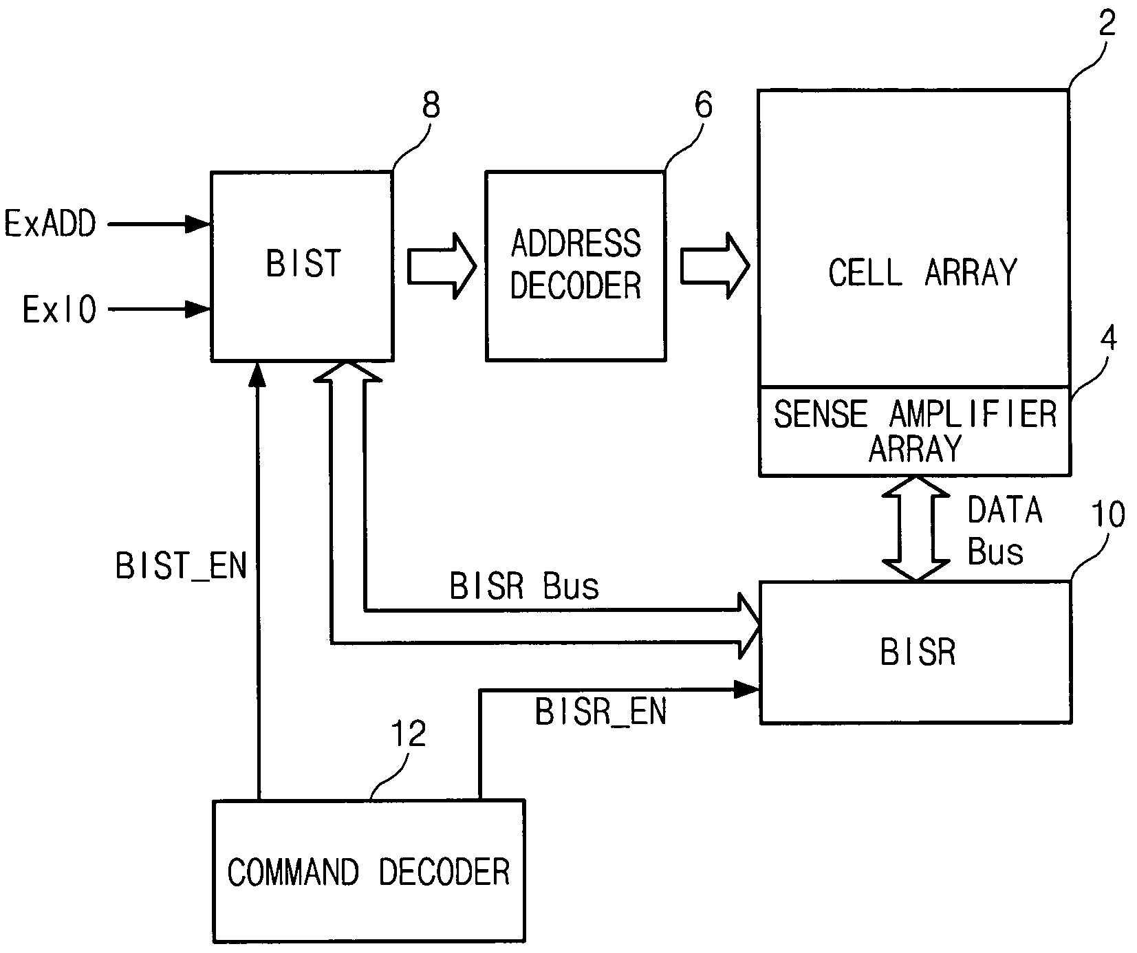
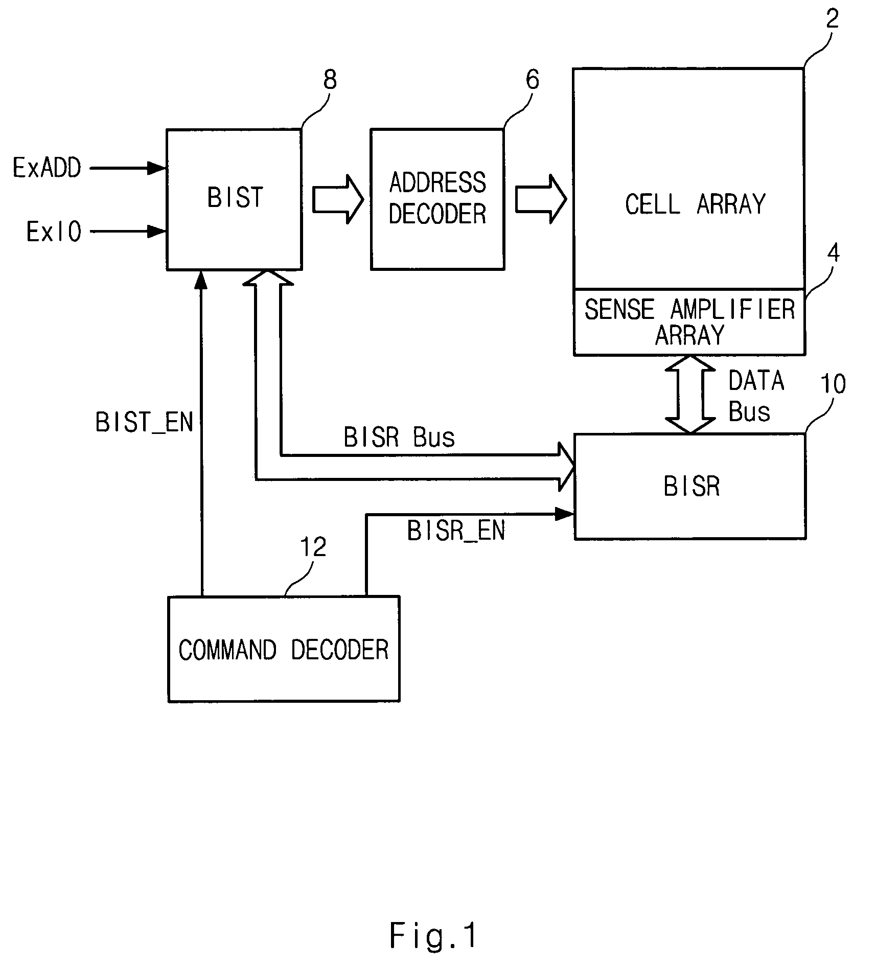
[0026]FIG. 1 is a block diagram illustrating a semiconductor memory device according to an embodiment of the present invention.

[0027]In this embodiment, a semiconductor memory device comprises a cell array 2, a sense amplifier array 4, an address decoder 6, a BIST 8, a BISR 10 and a command decoder 12.

[0028]The BIST 8 receives an external address ExADD and external data ExIO which may be provided by an external tester via a lead on the memory device.

[0029]The BIST 8 and the BISR 10 are connected by a BISR bus, and the BISR 10 and the sense amplifier 4 are connected by a data bus.

[0030]The command decoder 12 generates enable signals BIST_EN and BISR_EN to control the operations of the BIST 8 and the BISR 10. As a result, a BIST mode and a BISR mode can be individually ...


PUM


Abstract

A semiconductor memory device having a test control circuit includes a cell array, a BIST (built-in self test) circuit adapted and configured to perform a BIST operation on the cell array, a BISR (built-in self repair) circuit adapted and configured to perform a BISR operation on the cell array, and a command decoder adapted and configured to generate a first control signal for selecting a BIST operation by the BIST circuit or a test by an external tester and a second control signal for controlling a BISR operation by the BISR circuit. As a result, a test by an external tester, a BIST (built-in self test) and a BISR (built-in self repair) are individually performed in response to an additional command signal.

Description

BACKGROUND OF THE INVENTION[0001]1. Field of the Invention[0002]The present invention generally relates to a semiconductor memory device, and more specifically concerns a memory device capable of being tested by an external tester or a Built-In Self Test (hereinafter, referred to as “BIST”) and including a Built-In Self Repair (hereinafter, referred to as “BISR”).[0003]2. Description of the Related Art[0004]In general, memory chip manufacturers perform a test on a memory at a manufacturing site.[0005]Users depend on reliability of a chip to perform a proper operation of their system.[0006]As a density and a linewidth of a memory cell in a memory chip are continuously reduced (currently, 0.5 micron or less), it is difficult to achieve a desired reliability.[0007]As a result, the object of the memory device manufacturers is to increase memory capacity without reduction of chip yield due to a mis-operation product.[0008]Before shipment of memory chips, the memory chips are tested to ve...

Claims


Application Information

Patent Timeline
Patent Type & Authority Patents(United States)
IPC IPC(8): G01R31/28G11C29/00
CPCG11C29/14G11C29/46G11C11/22G11C2029/0407G11C29/40G11C11/40
Inventor KANG, HEE BOKAHN, JIN HONG
Owner SK HYNIX INC
Learn More