Element for detecting the amount of lapping having a resistive film electrically connected to the substrate

a resistive film and element technology, applied in the direction of lapping machines, instruments, manufacturing tools, etc., can solve the problems of reducing the number of sliders that can be produced from a single wafer, affecting the measurement accuracy, so as to reduce the area for arranging pads

Active Publication Date: 2008-09-09
SAE MAGNETICS (HK) LTD
View PDF14 Cites 10 Cited by
  • Summary
  • Abstract
  • Description
  • Claims
  • Application Information

AI Technical Summary

Benefits of technology

[0011]An object of the present invention is to provide an element for detecting the amount of lapping of a magnetic field detecting sensor which enables a reduction in the area for arranging pads.
[0013]Since one end of the resistive film is grounded to the substrate, unlike prior art, there is no need to provide two pads that are connected to the respective ends of the resistive film. Only one pad which is connected to one end of the resistive film is required. The pad needs a certain amount of area to enable a connection with a wire for wire bonding or to enable a connection with a probe. Therefore, the fact that only one pad is needed means that it is possible to significantly reduce the area that is required for arranging a pad. Accordingly, it is possible to produce a larger number of stacked structures of layers which include magnetic field detecting sensors from a single wafer.
[0017]As described above, it is possible to halve the number of pads that are arranged according to the present invention. Accordingly, it is possible to provide an element for detecting the amount of lapping of a magnetic field detecting sensor which allows a reduction in the size of the area for arranging a pad.

Problems solved by technology

Also, this method is effective when accurate measurement of the element resistance is difficult due to what is called smearing, which is caused by lapping an element, such as a TMR (Tunnel Magneto Resistive) element.
However, an increase in the size of the spacing portions leads to a decrease in the number of sliders that can be produced from a single wafer.
This makes it difficult to provide two pads without significantly influencing the measurement.
However, it is difficult to provide pads for the last bar in the block, which may lead to deterioration in lapping accuracy.
Furthermore, it may be difficult to reduce the width of the spacing portions between adjacent bars.

Method used


Image

  • Element for detecting the amount of lapping having a resistive film electrically connected to the substrate
  • Element for detecting the amount of lapping having a resistive film electrically connected to the substrate
  • Element for detecting the amount of lapping having a resistive film electrically connected to the substrate

Examples


Embodiment Construction

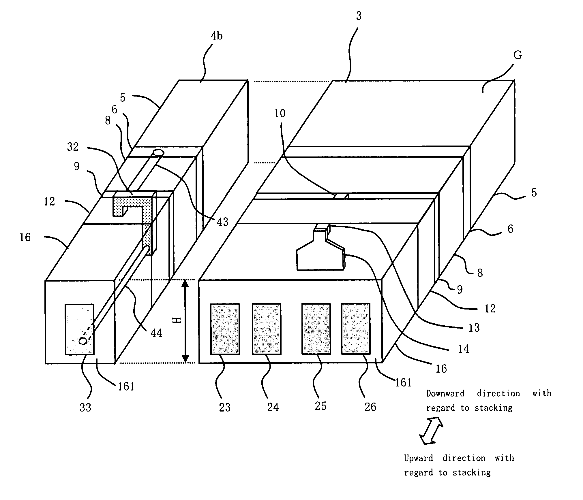
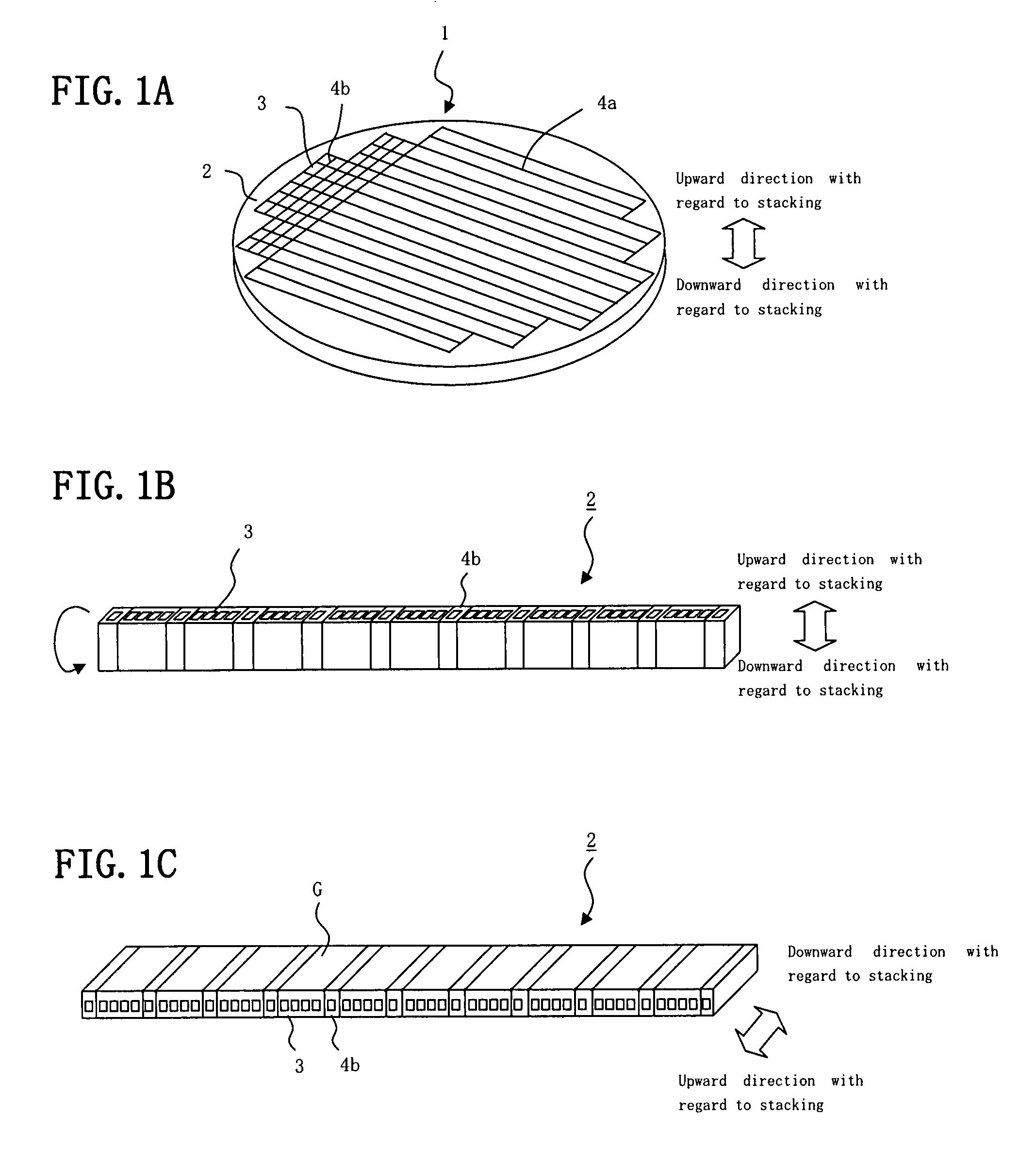
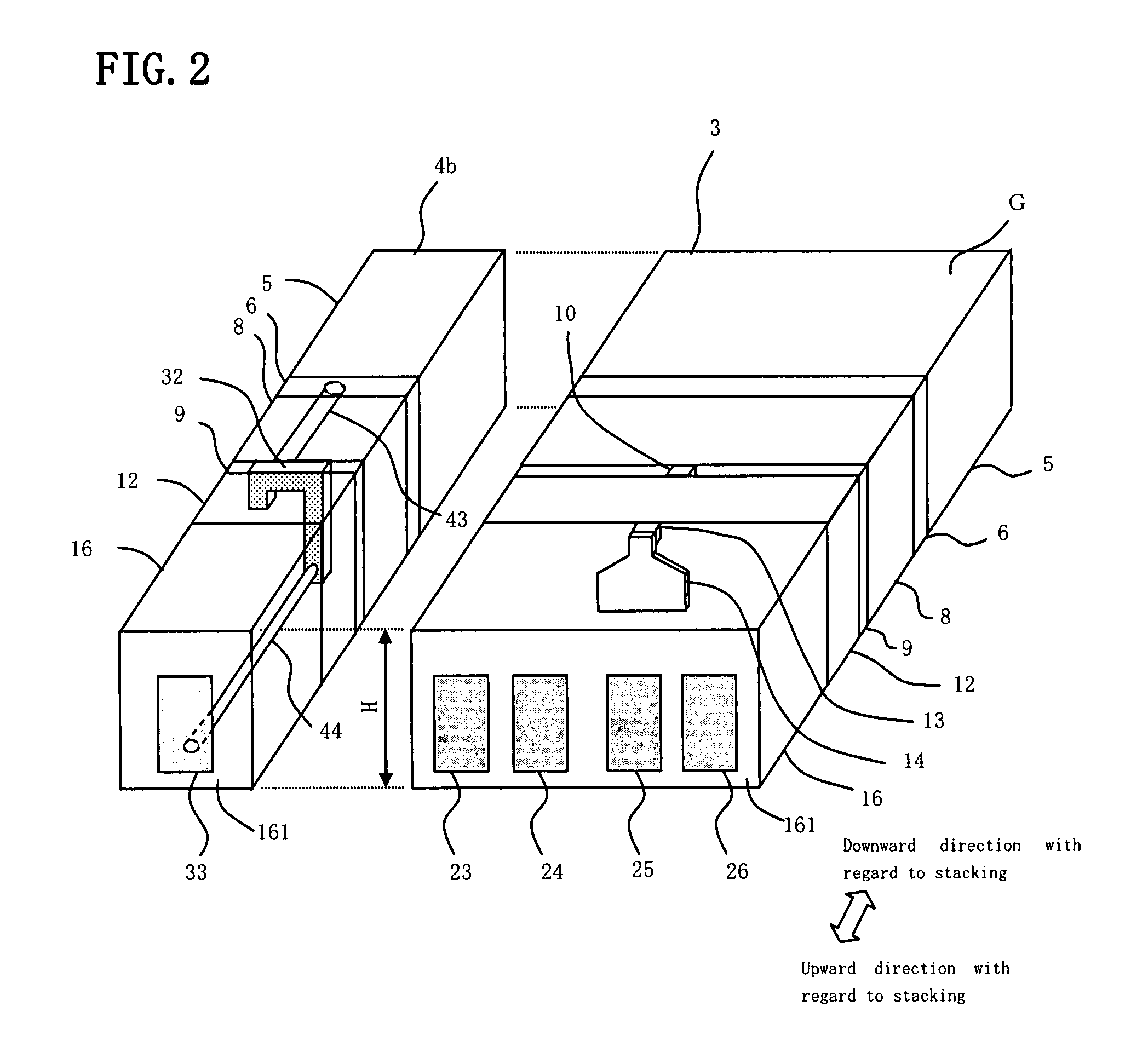
[0024]An element for detecting the amount of lapping in accordance with the present invention will be described with reference to the drawings. FIGS. 1A to 1C are perspective views of a wafer and bars having an element for detecting the amount of lapping in accordance with an embodiment of the present invention. FIG. 1A is a schematic view of a wafer, as viewed from the upper side of the wafer with regard to the direction of stacking (the direction is shown by the white arrow in the figure). Wafer 1 has a substrate, such as a silicon substrate, and many slider portions 3 which are two-dimensionally arranged on the substrate. Each slider portion 3 is formed into a slider that has a magnetic field detecting sensor (for example, MR element 10 which will be described later). Spacing portions 4a, 4b are formed on the periphery of each slider portion 3. FIG. 1B is a perspective view of a bar that is separated from the wafer by dicing, as, similar to FIG. 1, viewed from the upper side of t...


PUM

PropertyMeasurementUnit
heightaaaaaaaaaa
heightaaaaaaaaaa
widthaaaaaaaaaa

Abstract

An element for detecting an amount of lapping of a stacked structure that includes a substrate and a magnetic field detecting sensor is provided. The element comprises: a resistive film that is arranged on a lapping surface of the stacked structure, the resistive film being exposed at the lapping surface together with the magnetic field detecting sensor, wherein the resistive film has a resistance value that varies depending on the amount of lapping; and a pad for measuring the resistance value, wherein the pad is formed on a surface of the stacked structure, the surface being other than the lapping surface, and wherein the pad is electrically connected to one end of the resistive film. Another end of the resistive film is electrically connected to the substrate.

Description

[0001]The present application is based on, and claims priority from, J.P. Application No. 2006-162211, filed on Jun. 12, 2006, the disclosure of which is hereby incorporated by reference herein in its entirety.BACKGROUND OF THE INVENTION[0002]1. Field of the Invention[0003]The present invention relates to an element for detecting the amount of lapping that is used in a lapping step of a stacked structure of layers, a wafer that has such an element, and a method for lapping a stacked structure of layers using such an element. The present invention particularly relates to the structure of an element for detecting the amount of lapping that is used in a lapping step of a thin film magnetic head that is used in a hard disk drive.[0004]2. Description of the Related Art[0005]A thin film magnetic head that is used in a hard disk drive is manufactured through various manufacturing processes, which are generally classified into a wafer process, a slider process, and an assembly process. The ...

Claims


Application Information

Patent Timeline
Patent Type & Authority Patents(United States)
IPC IPC(8): B24B49/00B24B37/013B24B49/10G11B5/31G11B5/39
CPCG01R33/07G01R33/09G01R33/12Y10T29/49041Y10T29/49046
Inventor FUKUROI, OSAMU
Owner SAE MAGNETICS (HK) LTD
Why Eureka
Try Eureka