Semiconductor light emitting device capable of increasing its brightness

a technology of semiconductor light and light emitting device, which is applied in the direction of semiconductor devices, basic electric elements, electrical appliances, etc., can solve the problems of inconvenient heat generation of plastic encapsulants by heat from semiconductors, semiconductor devices deteriorating electrical properties, and resin deterioration under heat, so as to facilitate molding operation, improve reliability of semiconductor light emitting devices, easy and shorten wiring

Inactive Publication Date: 2008-09-30
SANKEN ELECTRIC CO LTD
View PDF20 Cites 54 Cited by
  • Summary
  • Abstract
  • Description
  • Claims
  • Application Information

AI Technical Summary

Benefits of technology

[0017]The method for producing a semiconductor light emitting device according to the present invention comprises the steps of providing an assembly (10) which includes a metallic support plate (1) and a light-reflective reflector (3) attached on the support plate (1); mounting a semiconductor light emitting element (2) on the support plate (1); electrically connecting the light emitting element (2) to wiring conductor (5); setting the support plate (1) and reflector (3) in a cavity (23) of a forming mold (20) and clamping the support plate (12) and reflector (3) between upper and lower mold halves (21, 22) of the forming mold (20); and supplying a liquid resin into the cavity (23) of the forming mold (20) to form a plastic encapsulant (6). As the support plate (12) and reflector (3) are clamped between upper and lower mold halves (21, 22) of the forming mold (20), liquid resin is prevented from entering the interior of the reflector (3) to facilitate the molding operation.
[0018]The semiconductor light emitting device according to the present invention, comprises a support plate (1); a light-reflective reflector (3) mounted on the support plate (1) and formed with a hole (3a) upwardly diverging; and a semiconductor light emitting element (2) mounted on the support plate (1) within the hole (3a) of the reflector (3). The reflector (3) has a ledge (3d) connected to a wiring conductor (5) to electrically connect the light emitting element (2) and wiring conductor (5) through the ledge (3d) for easy and shortened wiring and improvement in reliability of semiconductor light emitting device. Also, the ledge (3d) can be embedded and securely fixed in the plastic encapsulant (6) by a molding process. In addition, the reflecting surface (3c) can be formed with a smaller diameter and with an increased height to enhance the directivity and axial brightness of light from the light emitting device.
[0019]The reflector for semiconductor light emitting device according to the present invention is secured on the support plate (1) surrounding the semiconductor light emitting element (2) on the support plate (1) to reflect upwardly light from the light emitting element (2). The reflector comprises a reflector block (3b) formed with a hole (3a) for defining a reflecting surface (3c) with the upwardly enlarging inner diameter and a notch (3k) formed on the reflector block (3b) between the hole (3a) and an outer side wall (3m) or between the light emitting element (2) and wiring conductor (5). A lead wire (8) passes through the notch (3k) to electrically connect the light emitting element (2) and wiring conductor (5) by substantially straight extending lead wire (8) of the minimum span while the structure prevents the lead wire (8) from being deformed and facilitates connection between the light emitting element (2) and wiring conductor (5) by the lead wire (8). Avoidance of the lead wire (8) along an elevated path over an upper surface of the reflector (3) represses disconnection or breaking of the lead wire (8) to better reliability of the semiconductor light emitting device. Reduction of inner diameter of the reflecting surface (3c) and increase of height of the reflector (3) serve to gain improved light directivity and axial brightness of the reflector (3). Moreover, shorter inner diameter of the reflecting surface (3c) is effective for downsizing the reflector (3).
[0020]The semiconductor light emitting device according to the present invention, comprises a support plate (1); a light-reflective reflector (3) having a reflector block (3b) which is mounted on the support plate (1) or integrally formed with the support plate (1), the reflector (3) being formed with a hole (3a) upwardly expanding; a semiconductor light emitting element (2) mounted on the support plate (1) within the hole (3a) of the reflector (3); a first wiring conductor (4) electrically connected to one electrode of the light emitting element (2); a second wiring conductor (5) electrically connected to the other electrode of the light emitting element (2) through a lead wire (8); and a plastic encapsulant (6) for sealing at least the hole (3a) of the reflector (3). The reflector (3) also has a notch (3k) which passes through the reflector block (3b) between the hole (3a) and an outer side wall (3m) and between the light emitting element (2) and wiring conductor (5). The lead wire (8) passes through the notch (3k) to electrically connect the light emitting element (2) and wiring conductor (5) by substantially straight extending lead wire (8) of the minimum span while the structure prevents the lead wire (8) from being deformed and facilitates connection between the light emitting element (2) and wiring conductor (5) by the lead wire (8). Avoidance of the lead wire (8) along an elevated path over an upper surface of the reflector (3) represses disconnection or breaking of the lead wire (8) to better reliability of the semiconductor light emitting device. Reduction of inner diameter of the reflecting surface (3c) and increase of height of the reflector (3) serve to gain improved light directivity and axial brightness of the reflector (3). In another embodiment of the present invention, the notch (3k) of the reflector (3) provides a passage for liquid resin to fill the hole (3a) of the reflector (3) with the liquid resin.

Problems solved by technology

To this end, new high power light emitting semiconductors have already been developed to produce a high intensity light when relatively large electric current for example more than 350 mA is supplied to the light emitting semiconductors, however, they have caused the following various problems.
Specifically, when the element is activated with a large electric current over 350 mA, it is heated so that a surface of semiconductor may reach a temperature above 150° C., and therefore, plastic encapsulant is also inconveniently awfully heated by heat from the semiconductor.
Such a resin tends to deteriorate under heat because it contains less additive amount of heat-resistible compound unlike a package for a power transistor or the like.
When some foreign matter penetrates semiconductor through the gaps, the semiconductor device deteriorates the electric properties with degradation of product reliability.
Furthermore, adhesive force of encapsulant is lowered too much, lead terminals are detached from encapsulant to such an extent of current breaking between semiconductor and lead terminals.
Such an arrangement is likely to cause deformation, suspension or inclination of lead wire 150 upon molding of plastic material, which may result in short circuit or breaking accident of lead wire 150.

Method used


Image

  • Semiconductor light emitting device capable of increasing its brightness
  • Semiconductor light emitting device capable of increasing its brightness
  • Semiconductor light emitting device capable of increasing its brightness

Examples


Embodiment Construction

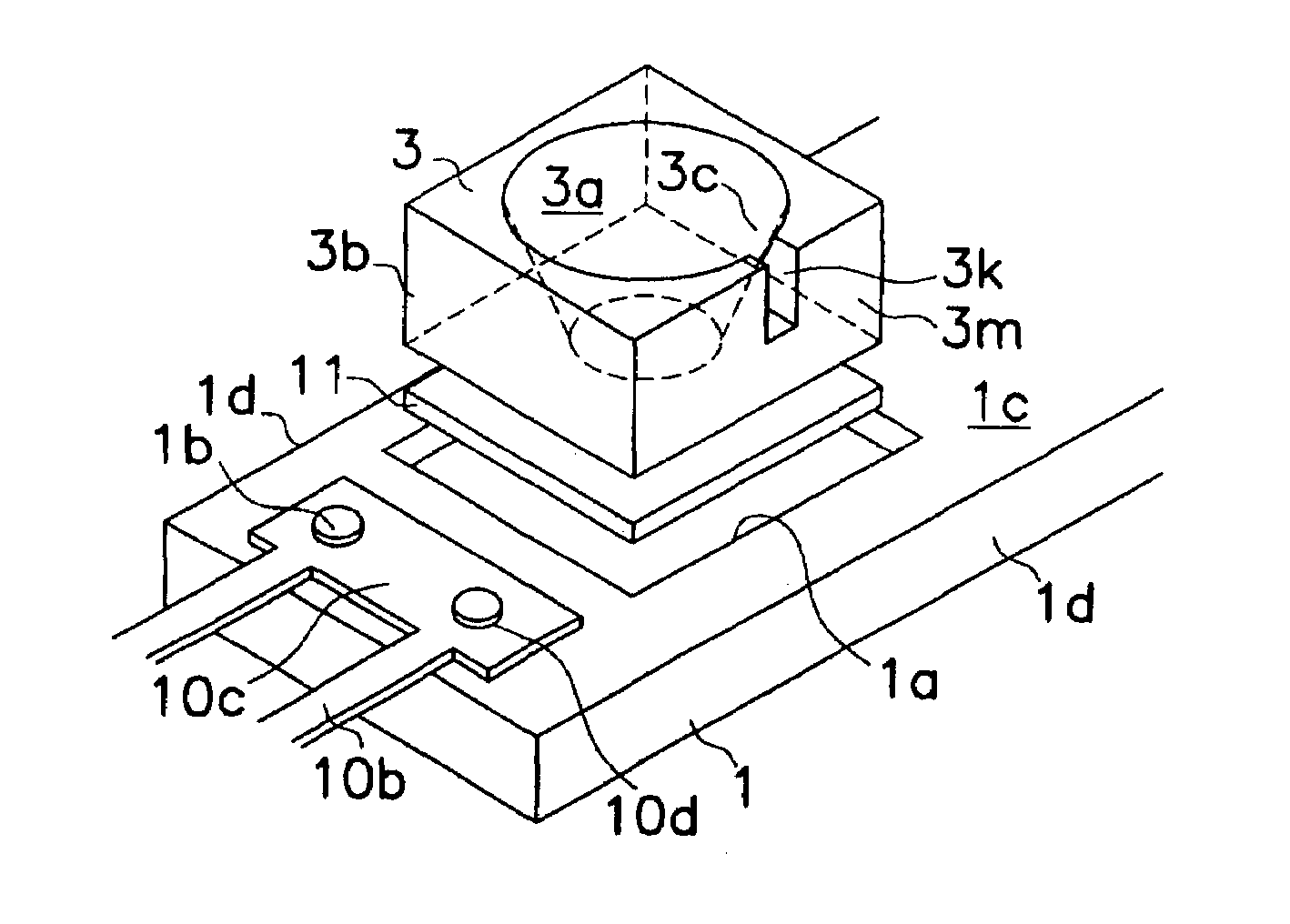
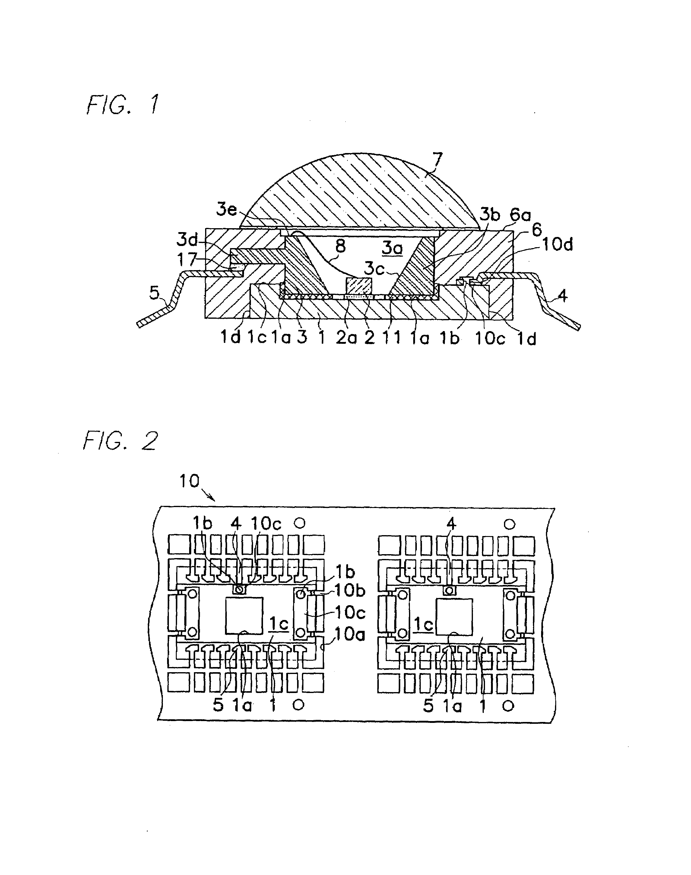
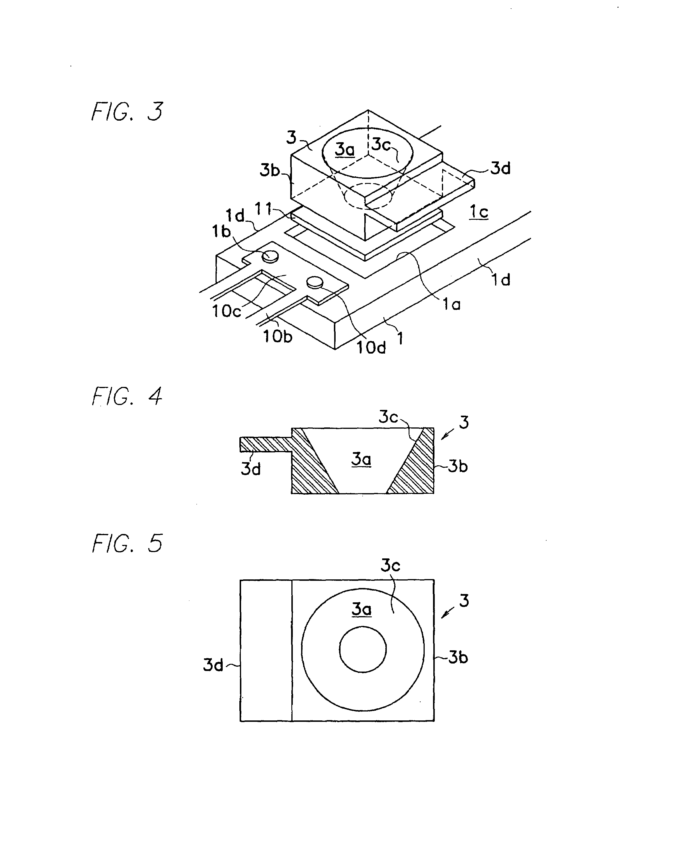
[0059]A semiconductor light emitting device shown in FIG. 1 comprises a metallic support plate 1 formed with a recess 1a; a light-reflective reflector 3 mounted in recess la of support plate 1 in electrically insulating relation to support plate 1, and formed with a hole 3a upwardly expanding; a light emitting diode 2 mounted on recess la of support plate 1 within hole 3a of reflector 3, one electrode (a bottom electrode) of the light emitting diode 2 being electrically connected to support plate 1; a first wiring conductor 4 electrically connected to support plate 1; a second wiring conductor 5 electrically connected to the other electrode (a top electrode) of light emitting diode 2; a lead wire 8 for electrically connecting light emitting diode 2 and reflector 3; a heat-resistible plastic encapsulant 6 for encapsulating outer periphery of reflector 3, upper and side surfaces 1c, 1d of support plate 1, each inner end of first and second wiring conductors 4, 5; and a lens 7 for cove...


PUM


Abstract

A semiconductor light emitting device comprises a metallic support plate 1; a light-reflective reflector 3 mounted on the support plate 1 and formed with a hole 3a; a semiconductor light emitting element 2 mounted on the support plate 1 within the hole 3a of the reflector 3, and a plastic encapsulant 6 for sealing an outer periphery of the reflector 3 and an upper surface 1c of the support plate 1. As the reflector 3 is electrically connected to a wiring conductor 5 or a lead wire 8 extends through a notch 3k formed in the reflector 3 to electrically connect the semiconductor light emitting element 2 and wiring conductor 5, wiring span of the lead wire 8 can be shortened to prevent deformation of the lead wire 8. Simultaneously, diameter of the reflective surface 3c in the reflector 3 is reduced and height of the reflector 3 is increased to improve directivity and axial brightness of light from the semiconductor light emitting device. Also, formation of the hole 3a effectively prevents further thermal degradation of heat-resistible plastic encapsulant 6 or other resin components.

Description

TECHNICAL FIELD[0001]This invention relates to a semiconductor light emitting device and a reflector for such a semiconductor light emitting device, in particular a semiconductor light emitting device, a method for producing the same and a reflector for the semiconductor light emitting device capable of avoiding harmful effect by heat and deformation of a lead wire connected to a light emitting element when they may occur with heavy electric current through the light emitting device.BACKGROUND OF THE INVENTION[0002]Japanese Patent Disclosure No. 11-340517 discloses a semiconductor light emitting device which comprises an insulating substrate formed with wiring conductors, a semiconductor element attached on a main surface of the substrate, a reflector (a light reflecting plate) surrounding the semiconductor element on the substrate, and a light-transmittable plastic encapsulant for encapsulating the semiconductor element and reflector. FIG. 36 illustrates a known semiconductor light...

Claims


Application Information

Patent Timeline
Patent Type & Authority Patents(United States)
IPC IPC(8): H01L33/00H01L33/58H01L33/60H01L33/62H01L33/64
CPCH01L33/62H01L33/647H01L33/60H01L33/486H01L2224/16245H01L33/642H01L2224/48091H01L2224/48247H01L2224/73265H01L2924/01057H01L2924/01078H01L2924/01079H01L2924/3025H01L2924/12041H01L2924/01019H01L2924/00014
Inventor OYAMA, TOSHIHIKOKOBAYASHI, NOBUOOSAWA, HIDEYUKIOGATA, TOSHIO
Owner SANKEN ELECTRIC CO LTD
Why Eureka
Try Eureka