Method of wafer laser processing using a gas permeable protective tape

a protective tape and laser processing technology, applied in the field of wafer laser processing, can solve the problems of reducing the service life so as to eliminate the decline in the wafer holding force of the chuck table

Active Publication Date: 2008-10-14
DISCO CORP
View PDF8 Cites 112 Cited by
  • Summary
  • Abstract
  • Description
  • Claims
  • Application Information

AI Technical Summary

Benefits of technology

[0006]It is an object of the present invention to provide a wafer laser processing method capable of removing the influence of bubbles even when a protective tape affixed to a wafer absorbs the energy of a laser beam applied to the wafer to produce the bubbles.
[0012]In the present invention, since the protective tape affixed to one side of the wafer has gas permeability, bubbles produced when the protective tape is heated by the energy of the laser beam do not accumulate in a space between the protective tape and the wafer and are discharged through the protective tape. Therefore, the bubbles do not accumulate in the space between the protective tape and the wafer and do not raise the wafer. Consequently, the displacement of the focusing point of the laser beam caused by the rise of the wafer held on the chuck table by the bubbles can be prevented and a decline in the wafer holding force of the chuck table is eliminated.

Problems solved by technology

Since the sapphire substrate and the lithium tantalite substrate have high Mohs hardness, cutting with the above cutting blade is not always easy.
As a result, a problem arises in that the wafer held on the chuck table is slightly raised by the bubbles, whereby the focusing point of the laser beam is displaced and a uniform deteriorated layer cannot be formed thereby.
Further, there is another problem in that since the wafer held on the chuck table is slightly raised by the bubbles, the wafer holding force of the chuck table weakens.

Method used


Image

  • Method of wafer laser processing using a gas permeable protective tape
  • Method of wafer laser processing using a gas permeable protective tape
  • Method of wafer laser processing using a gas permeable protective tape

Examples


Embodiment Construction

[0021]Preferred embodiments of the wafer laser processing method of the present invention will be described hereinunder with reference to the accompanying drawings.

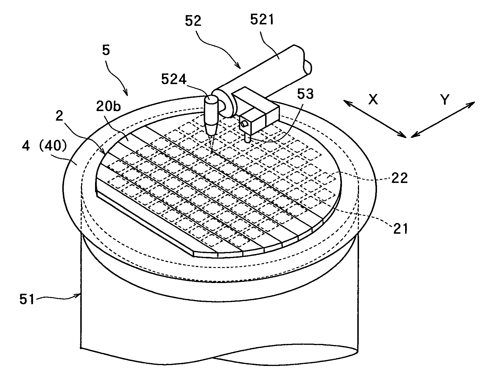
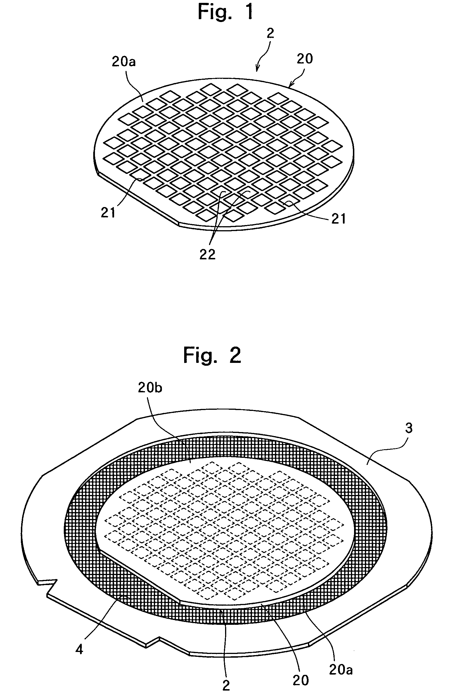
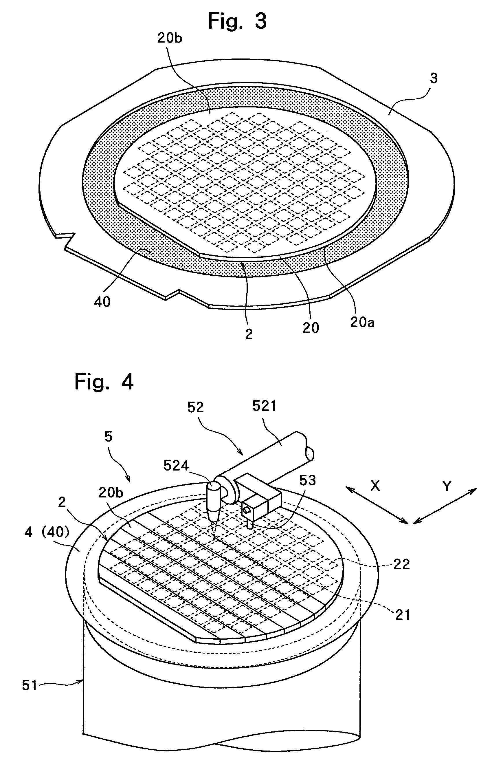
[0022]FIG. 1 is a perspective view of an optical device wafer as a wafer to be processed by the laser processing method of the present invention. In the optical device wafer 2 shown in FIG. 1, optical devices 22 comprising laminated gallium nitride-based compound semiconductors are formed in a plurality of areas sectioned by dividing lines 21 on the front surface 20a of a sapphire substrate 20. A description is subsequently given of a wafer laser processing method for carrying out laser processing along the dividing lines 21 of this optical device wafer 2.

[0023]To carry out laser processing along the dividing lines 21 of the above-described optical device wafer 2, the step of affixing a protective tape having gas permeability to one surface of the above optical device wafer 2 is first carried out. This protective tape aff...


PUM

PropertyMeasurementUnit
diameteraaaaaaaaaa
diameteraaaaaaaaaa
gas permeabilityaaaaaaaaaa

Abstract

A laser processing method for forming a deteriorated layer, which has been once molten and then re-solidified, in the inside of a wafer by applying a pulse laser beam capable of passing through the wafer to the wafer along a dividing line formed on the wafer, comprising: a protective tape affixing step for affixing a protective tape having gas permeability to one side of the wafer; a wafer holding step for holding the wafer having the protective tape affixed thereto on the chuck table of a laser beam machine in such a manner that the surface side onto which the protective tape has been affixed comes into contact with the chuck table; and a laser beam application step for applying a pulse laser beam capable of passing through the wafer from the other surface side of the wafer held on the chuck table with its focusing point set to a position near the one surface of the wafer to form the deteriorated layer exposed to the one surface along the dividing line in the inside of the wafer.

Description

FIELD OF THE INVENTION[0001]The present invention relates to a wafer laser processing method for forming a deteriorated layer in the inside of a wafer by applying a pulse laser beam capable of passing through the wafer along a dividing line formed on the wafer.DESCRIPTION OF THE PRIOR ART[0002]In the production process of a semiconductor device, a plurality of areas are sectioned by dividing lines called “streets” arranged in a lattice pattern on the front surface of a substantially disk-like semiconductor wafer, and a circuit such as IC or LSI is formed in each of the sectioned areas. Individual semiconductor chips are manufactured by cutting this semiconductor wafer along the streets to divide it into the areas in which the circuit is formed. An optical device wafer comprising optical devices comprising laminated gallium nitride-based compound semiconductors formed in a plurality of areas sectioned by dividing lines on the front surface of a sapphire substrate or a wafer comprisin...

Claims


Application Information

Patent Timeline
Patent Type & Authority Patents(United States)
IPC IPC(8): H01L21/00B23K26/364B23K26/38B23K26/40B23K101/40H01L21/301H01L21/46H01L21/68H01L21/78
CPCB23K26/0057H01L21/6835H01L21/78B23K2201/40H01L2221/6834B23K26/53B23K2101/40
Inventor NAGAI, YUSUKE
Owner DISCO CORP
Why Eureka
Try Eureka