Integration schemes for fabricating polysilicon gate MOSFET and high-K dielectric metal gate MOSFET

a technology of dielectric metal gate mosfet and polysilicon gate mosfet, which is applied in the direction of semiconductor devices, electrical devices, transistors, etc., can solve the problem that the improvement of pmosfet performance may not be sufficient to justify associated incremental cos

Active Publication Date: 2008-10-14
GLOBALFOUNDRIES US INC
View PDF20 Cites 11 Cited by
  • Summary
  • Abstract
  • Description
  • Claims
  • Application Information

AI Technical Summary

Problems solved by technology

Since the use of a metal gate electrode with a high-K dielectric often introduces additional challenging, and oftentimes costly, processing steps, improvement of device performance through use of a metal gate electrode needs to be evaluated against the cost of the additional processes.
For example, performance of NMOSFETs may improve significantly with the use of a metal gate electrode and a high-K dielectric to justify the associated additional cost while improvement of performance of PMOSFETs may not be sufficient to justify associated incremental cost.

Method used


Image

  • Integration schemes for fabricating polysilicon gate MOSFET and high-K dielectric metal gate MOSFET
  • Integration schemes for fabricating polysilicon gate MOSFET and high-K dielectric metal gate MOSFET
  • Integration schemes for fabricating polysilicon gate MOSFET and high-K dielectric metal gate MOSFET

Examples


Embodiment Construction

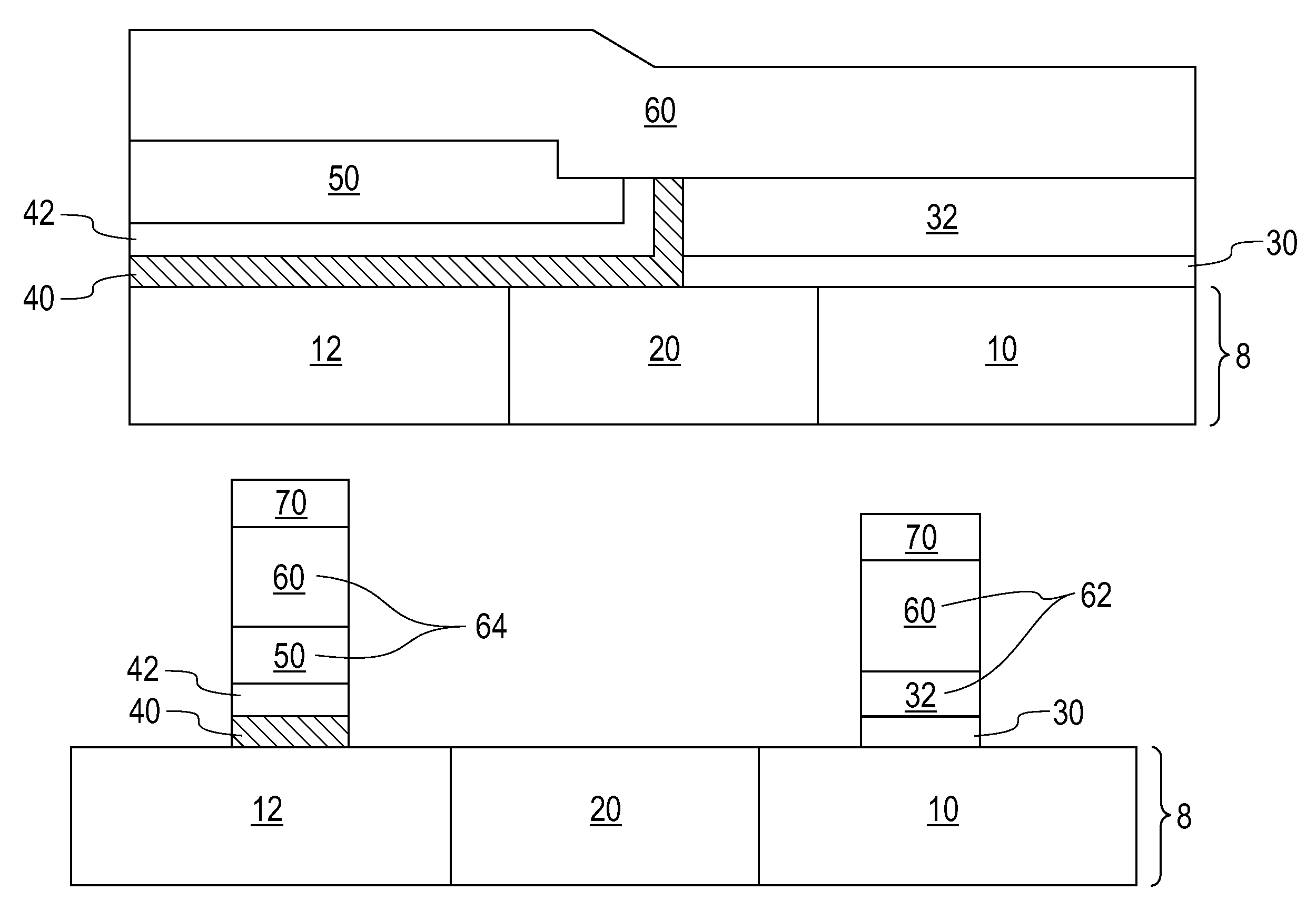
[0054]As stated above, the present invention relates to methods of manufacturing a semiconductor structures with at least one polysilicon gate electrode and at least one high-K dielectric metal gate electrode, which will now be described in greater detail by referring to the drawings that accompany the present application.

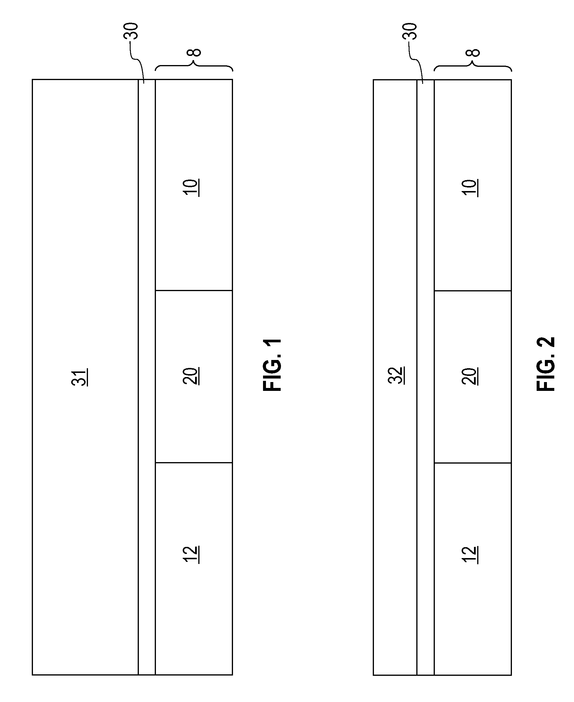
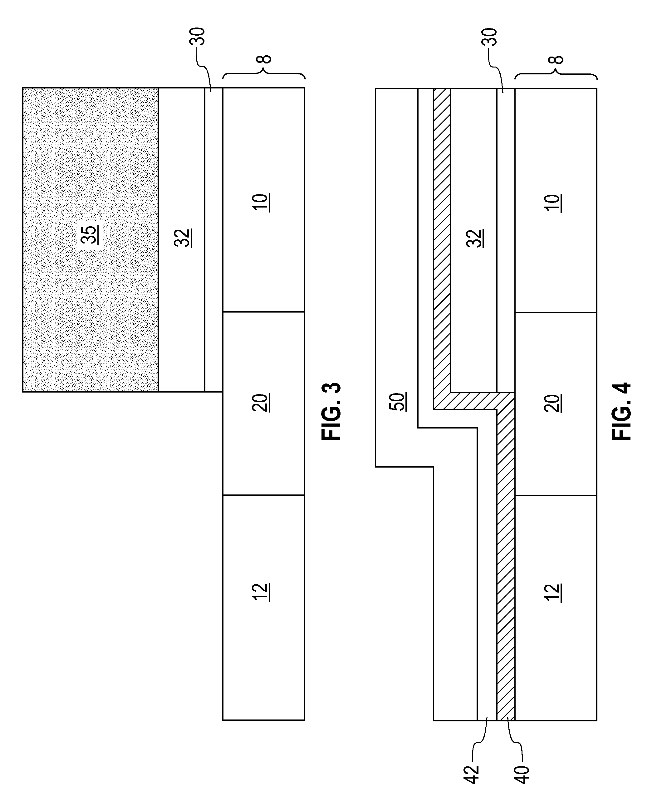
[0055]According to FIGS. 1-6, a series of vertical cross-sectional views demonstrating formation of an exemplary semiconductor structure with a polysilicon gate electrode, a high-K dielectric metal gate electrode, and shallow trench isolation are sequentially shown. FIGS. 1-6 are common processing steps according to the four embodiments of the present invention to be shown below. The non-limiting four embodiments of the present invention are shown for demonstration of the practicability of the present invention and obvious alterations and variations of these methods are implied in the present disclosure. Manufacture of more than two gate electrodes according to the...


PUM


Abstract

Multiple integration schemes for manufacturing dual gate semiconductor structures are disclosed. By employing the novel integration schemes, polysilicon gate MOSFETs and high-k dielectric metal gate MOSFETs are formed on the same semiconductor substrate despite differences in the composition of the gate stack and resulting differences in the etch rates. A thin polysilicon layer is used for one type of gate electrodes and a silicon-containing layer are used for the other type of gate electrodes in these integration schemes to balance the different etch rates and to enable etching of the two different gate stacks.

Description

FIELD OF THE INVENTION[0001]The present invention relates to methods of fabricating semiconductor structures, and particularly to methods of fabricating semiconductor structures having a polysilicon gate MOSFET and a high-K dielectric metal gate MOSFET on the same semiconductor substrate.BACKGROUND OF THE INVENTION[0002]Enhancement of complementary metal oxide semiconductor (CMOS) circuit requires improvement in the performance of both the p-type metal oxide semiconductor field effect transistors (PMOSFETs) and n-type metal oxide semiconductor field effect transistors (NMOSFETs). While the same material and processing steps were shared between PMOSFETs and NMOSFETs in the past, recent trends in high performance PMOSFETs and NMOSFETs show increased use of different materials and different processing steps among the two types of transistors.[0003]An example in which differences in the manufacture of the transistors are preferred is in the selection of the gate conductor material. In t...

Claims


Application Information

Patent Timeline
Patent Type & Authority Patents(United States)
IPC IPC(8): H01L21/336
CPCH01L21/82345H01L21/823462H01L21/823842H01L21/823857H01L29/4966H01L21/28194H01L29/517
Inventor CHEN, TZE-CHIANGDORIS, BRUCE B.JAGANNATHAN, RANGARAJANYAN, HONGWENYANG, QINGYUNZHANG, YING
Owner GLOBALFOUNDRIES US INC
Why Eureka
Try Eureka