Analog buffer and driving method thereof, liquid crystal display apparatus using the same and driving method thereof

a technology of analog buffers and driving methods, applied in the field of analog buffers, can solve the problems of significant increase in power consumption, and achieve the effects of reducing power consumption, simplifying configuration, and simplifying configuration

Active Publication Date: 2008-10-14
LG DISPLAY CO LTD
View PDF10 Cites 14 Cited by
  • Summary
  • Abstract
  • Description
  • Claims
  • Application Information

AI Technical Summary

Benefits of technology

[0016]An object of the present invention is to provide an analog buffer and a method of driving an analog buffer having simplified configuration and reduced power consumption.
[0017]Another object of the present invention is to provide a liquid crystal display apparatus and a method of driving a liquid crystal display apparatus using an analog buffer having simplified configuration and reduced power configuration.

Problems solved by technology

The power consumption is significantly increased with increasing numbers of inverters.

Method used


Image

  • Analog buffer and driving method thereof, liquid crystal display apparatus using the same and driving method thereof
  • Analog buffer and driving method thereof, liquid crystal display apparatus using the same and driving method thereof
  • Analog buffer and driving method thereof, liquid crystal display apparatus using the same and driving method thereof

Examples


first embodiment

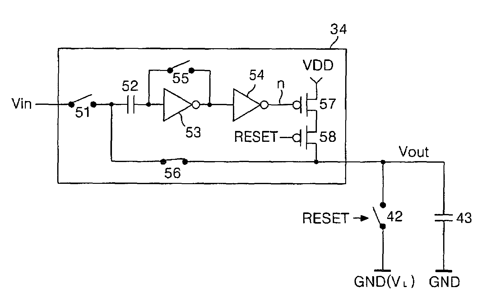
[0042]Referring to FIG. 5, an analog buffer 34 includes a first inverter 53, a first capacitor 52 connected in series between an input line and the first inverter 53, a first switch 51 connected between the input line and the first capacitor 52, a second switch 55 connected between an input terminal and an output terminal of the first inverter 53 and a third switch 56 connected between the input line and the output line of the analog buffer 34 which are used as the comparator 36 shown in FIG. 4. In addition, the analog buffer 34 shown in FIG. 5 further includes a second inverter 54 used as the controller 38 shown in FIG. 4 and a fourth switch 57, used as the constant current source 40 in FIG. 4, to control a conductive path between a first supply line VDD and an output line of the analog buffer 34 in accordance with an output signal of the second inverter 54. Herein, the fourth switch 57 and a fifth switch 58 are implemented with PMOS transistors as shown in FIG. 5.

[0043]In FIG. 5,...

second embodiment

[0051]Thus, in the analog buffer 44 according to the present invention, if the output voltage Vout on the data line becomes identical to the input voltage Vin, then a constant current path is cut-off. Accordingly, the power consumption in the analog buffer is reduced. Referring to FIG. 8B, if the output voltage Vout on the data line becomes identical to the input voltage Vin in the analog buffer shown in FIG. 7, it can be recognized that the power consumption in the analog buffer is remarkably reduced to a level of about 5 μW (microwatts).

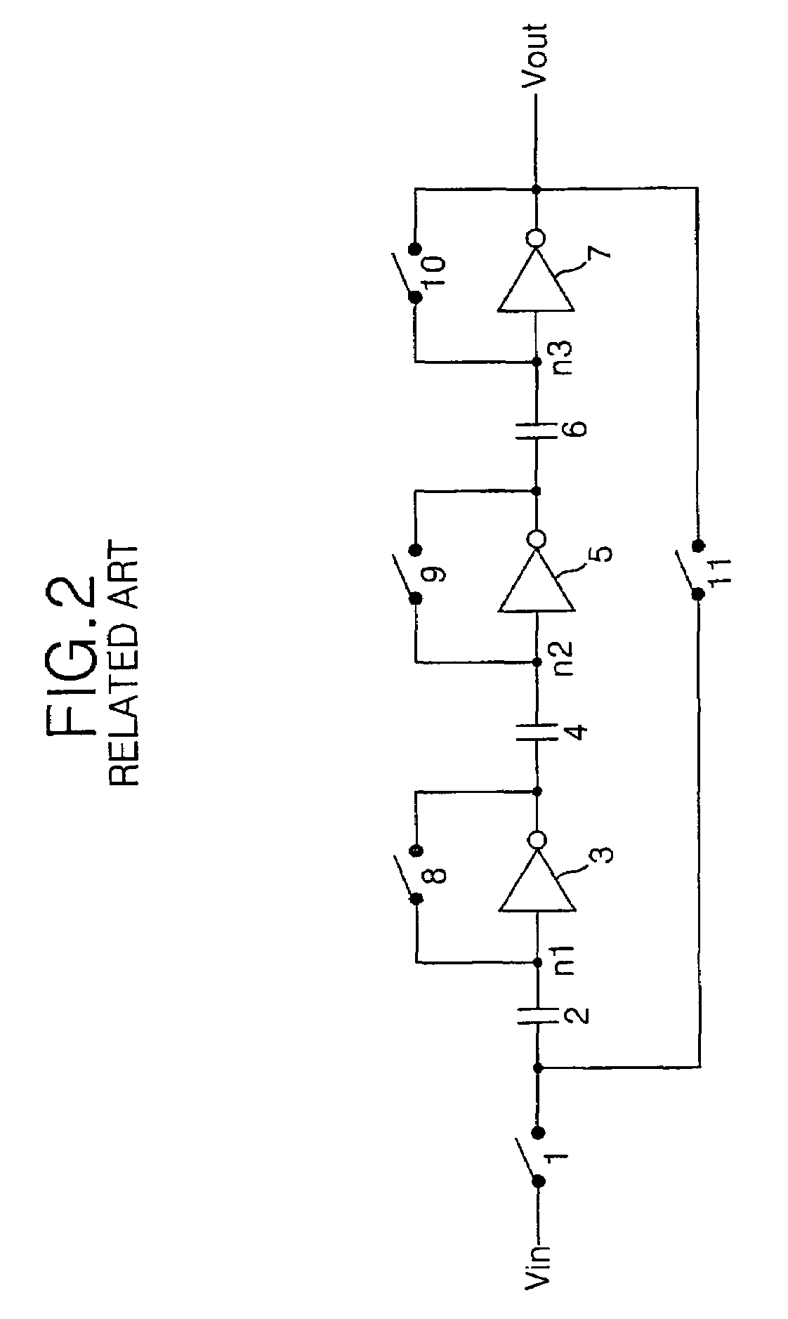
[0052]Also, the related art analog buffer shown in FIG. 2 uses an odd-number of inverters, e.g., three inverters with three capacitors. While the analog buffer 44 shown in FIG. 7 uses an even-number of elements, e.g., two inverters with a capacitor, thereby simplifying the circuit configuration of the analog buffer.

third embodiment

[0053]FIG. 9 shows a detailed circuit diagram of an analog buffer according to the present invention.

[0054]Referring to FIG. 9, an analog buffer 70 according to a third embodiment of the present invention further includes a second capacitor 79 connected in series to a feedback line through a third switch 80; a seventh switch 78 connected between an input terminal of a first capacitor 72 and an input line of a second supply voltage GND or VL; and an eighth switch 81 connected between a node between the second capacitor 79 and the third switch 80 and a line of the second supply voltage GND or VL. Herein, the feedback line is connected to a node between the first capacitor 72 and an input terminal of the first inverter 73.

[0055]In FIG. 9, a first, a second, a third, a fifth, a sixth, a seventh and a eighth switches 71, 77, 80, 76, 83, 78 and 81 are controlled by a reset pulse RESET. Among these switches, the first, the second, the sixth switch and the eighth switched 71, 77, 83 and 81 ...


PUM


Abstract

An analog buffer for buffering an input voltage to an output line is provided. The analog buffer includes a constant current source and a comparator. The constant current source supplies a constant current to the output line, and the comparator compares a voltage charged on the output line with the input voltage to turn-off the constant current source if it is determined that the voltage charged on the output line corresponding to the input voltage is buffered to the output line.

Description

[0001]This application claims the benefit of Korean Patent Application No. P2003-46067 filed in Korea on Jul. 8, 2003, which is hereby incorporated by reference.BACKGROUND OF THE INVENTION[0002]1. Field of the Invention[0003]The present invention relates to an analog buffer, and more particularly, to an analog buffer and a method of fabricating the same that are capable of reducing power consumption.[0004]2. Description of the Related Art[0005]A liquid crystal display device displays a picture by controlling the light transmittance of a liquid crystal material having a dielectric anisotropy using an electric field. To this end, the liquid crystal display device includes a liquid crystal panel having a pixel matrix and a drive circuit for driving the liquid crystal panel. As shown in FIG. 1, the liquid crystal display device includes a liquid crystal panel 2r having a pixel matrix, a gate driver 4r for driving gate lines GL1 to GLn of the liquid crystal panel 2r, a data driver 6r for...

Claims


Application Information

Patent Timeline
Patent Type & Authority Patents(United States)
IPC IPC(8): G09G3/36
CPCG09G3/3655G09G3/3688G09G2310/027G09G3/36
Inventor KIM, KEE JONGYOO, JUHN SUK
Owner LG DISPLAY CO LTD
Why Eureka
Try Eureka