Nitride-based compound semiconductor light emitting device
a light-emitting device and compound semiconductor technology, which is applied in the direction of semiconductor devices, basic electric elements, electrical equipment, etc., can solve the problems of sapphire substrate removal, hindering the formation of light-emitting devices, and conductive substrates that may peel off from the ohmic electrode, etc., and achieve good adhesion and high reliability.
- Summary
- Abstract
- Description
- Claims
- Application Information
AI Technical Summary
Benefits of technology
Problems solved by technology
Method used
Image
Examples
example 1
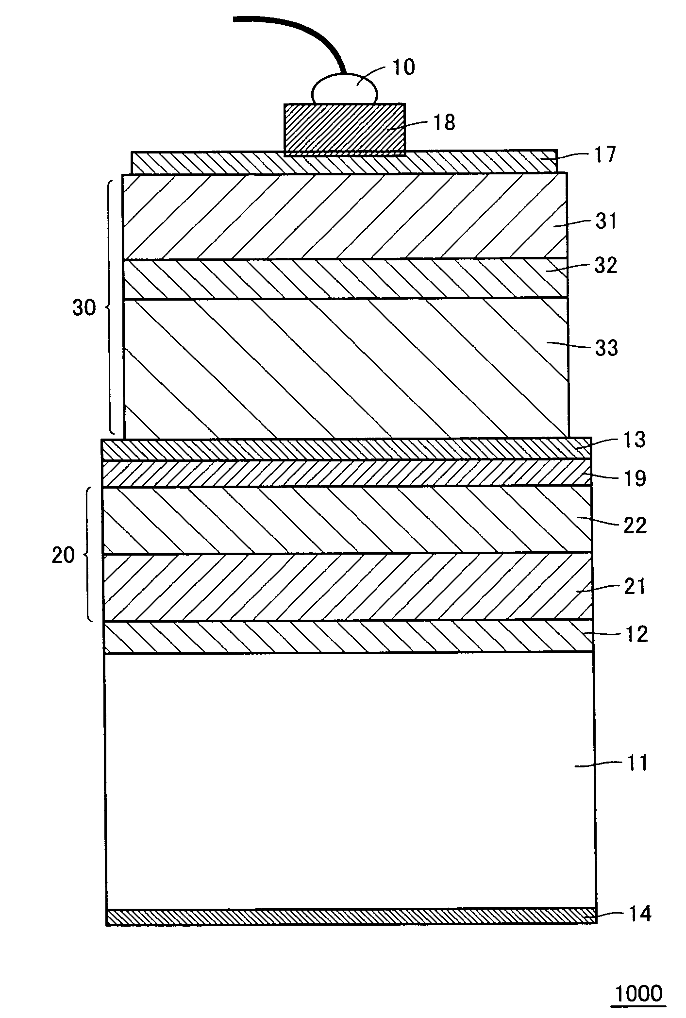
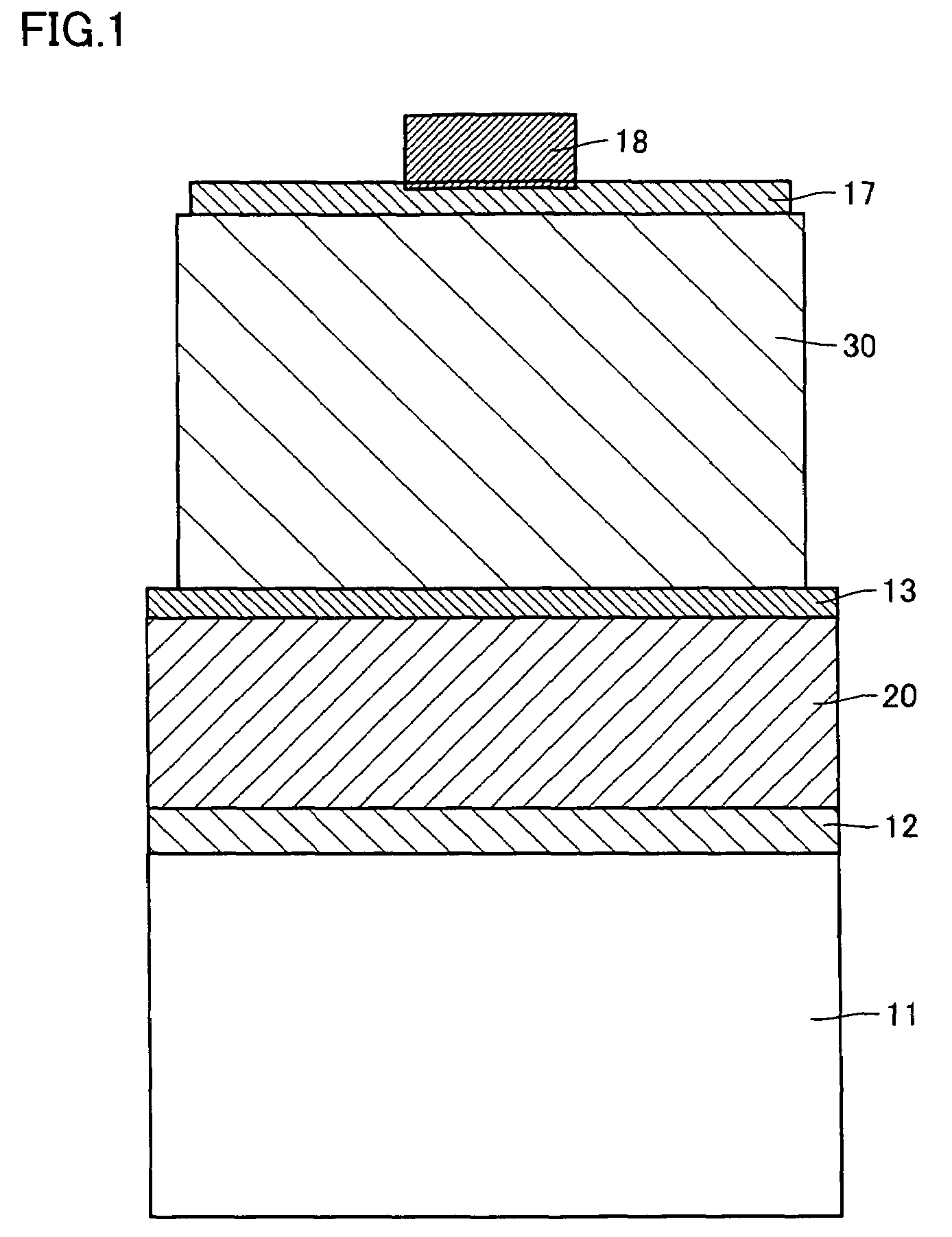
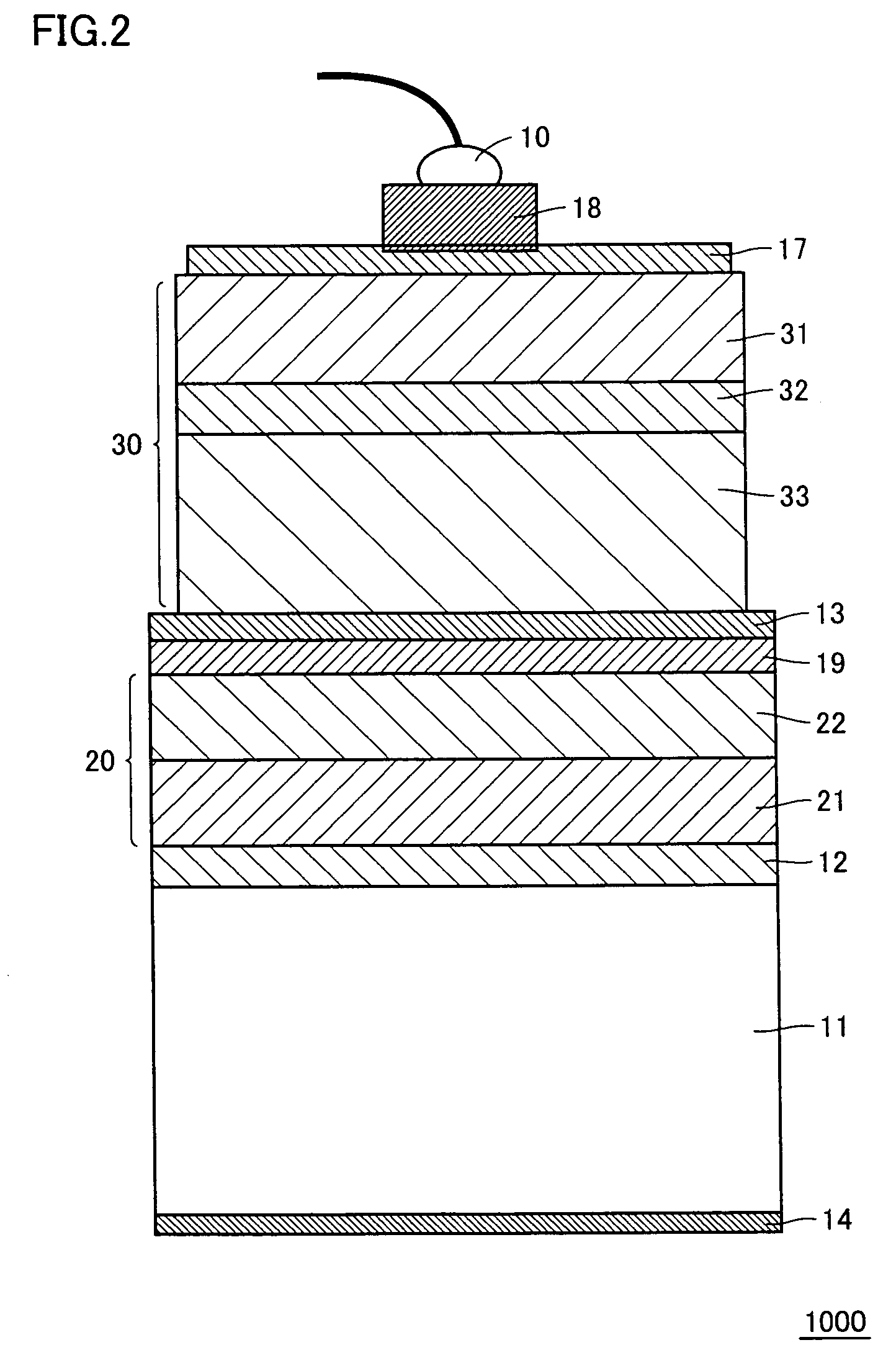
[0061]On a Si substrate serving as support substrate 11, a Ti (15 nm) / Al (150 nm) layer serving as first ohmic electrode 12 and an Au (3 μm) layer serving as first bonding metal layer 21 were formed in this order by EB evaporation.
[0062]Next, on a sapphire substrate serving as substrate 35, buffer layer 36, N-type nitride-based compound semiconductor layer 31, light emitting layer 32, and P-type nitride-based compound semiconductor layer 33 were formed successively by MOCVD. Specifically, a GaN buffer layer serving as buffer layer 36 was formed to a thickness of 20 nm, N-type nitride-based compound semiconductor layer 31 was formed to a thickness of 7 μm, a multi-quantum well (MQW) light emitting layer serving as light emitting layer 32 was formed to a thickness of 50 nm, and P-type nitride-based compound semiconductor layer 33 was formed to a thickness of 200 nm, successively in this order.
[0063]Next, on P-type nitride-based compound semiconductor layer 33, second ohmic electrode 1...
example 2
[0069]On a CuW substrate serving as support substrate 11, a Ti (15 nm) / Al (150 nm) layer serving as first ohmic electrode 12 and an Au (3 μm) layer serving as first bonding metal layer 21 were formed in this order by EB evaporation.
[0070]Next, on a sapphire substrate serving as substrate 35, buffer layer 36, N-type nitride-based compound semiconductor layer 31, light emitting layer 32, and P-type nitride-based compound semiconductor layer 33 were formed successively, using MOCVD. Specifically, a GaN buffer layer serving as buffer layer 36 was formed to a thickness of 20 nm, N-type nitride-based compound semiconductor layer 31 was formed to a thickness of 5 μm, an MQW light emitting layer serving as light emitting layer 32 was formed to a thickness of 50 nm, and P-type nitride-based compound semiconductor layer 33 was formed to a thickness of 200 nm, successively in this order.
[0071]Next, second ohmic electrode 13, reflecting metal layer 19, barrier metal layer 15 and second bonding ...
PUM
 Abstract
Description
Claims
Application Information


