Scalable shared network memory switch for an FPGA

Active Publication Date: 2008-10-21
XILINX INC
View PDF9 Cites 18 Cited by
  • Summary
  • Abstract
  • Description
  • Claims
  • Application Information

AI Technical Summary

Benefits of technology

[0009]Embodiments of the present invention provide a protocol agnostic cell based switch for communication between nodes of an FPGA. The switch can be used in conjunction with specific physical layer interfaces to implement switching interconnects between network nodes that support many different communication protocols, agnostic indicating that the protocol may be unknown and may or may not be a standard like Ethernet. Putting such a switch in an FPGA provides the user flexibility in terms of performance, tuning and customizable features of the design that are not available in ASIC devices.
[0010]The shared memory switch provided stores and retrieves data from the Block Random Access Memories (BRAMs) of an FPGA. The switch contains a set of input ports and output ports through which data can be sent and received. A scalable memory architecture is implemented allowing programmable scaling of the BRAM into an N×N memory structure, where N=number of input and output ports selected. Embodiments of the present invention use a very small amount of memory (BRAMs), even with programmable scaling, the memory size required having a linear dependence on the FPGA resources. In addition to BRAM, the switch architecture allows for linear scaling of other FPGA resources, such as shift register latches (SRLs) based on the number of ports selected. For example, resource usage=f(N) where f(N) is a simple linear function of N, N indicating the number of parts on the switch. The switch can further have parametrizable port data-paths (i.e., 16, 32, 64 bits) with a physical layer bus interface going into and out of every port.
[0011]The scalable memory is implemented by pipelining data and storing data pointers that identify BRAM storage locations for data in the N×N memory based on write time, rather than addressing. Pipelining and the elimination of addressing further provides a guaranteed latency for traffic (packets/cells) going from the input ports to the output ports of the network switch. Pipelining is further aided by a n

Problems solved by technology

A PCI express switch will not support other proto

Method used


Image

  • Scalable shared network memory switch for an FPGA
  • Scalable shared network memory switch for an FPGA
  • Scalable shared network memory switch for an FPGA

Examples


Embodiment Construction

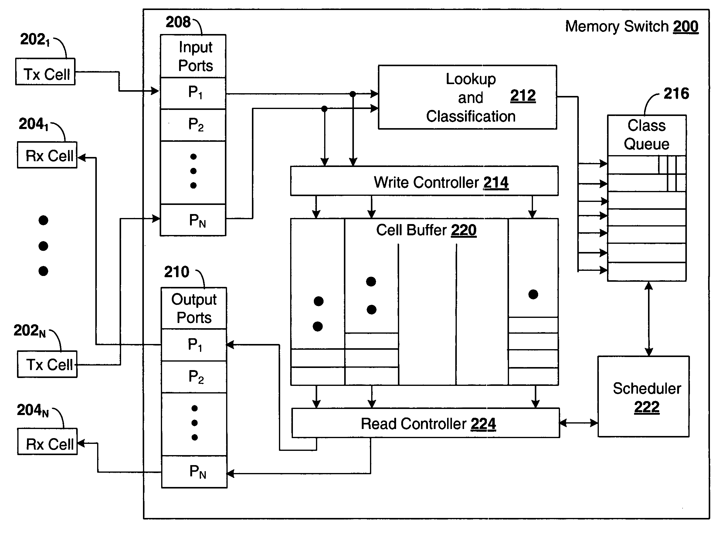
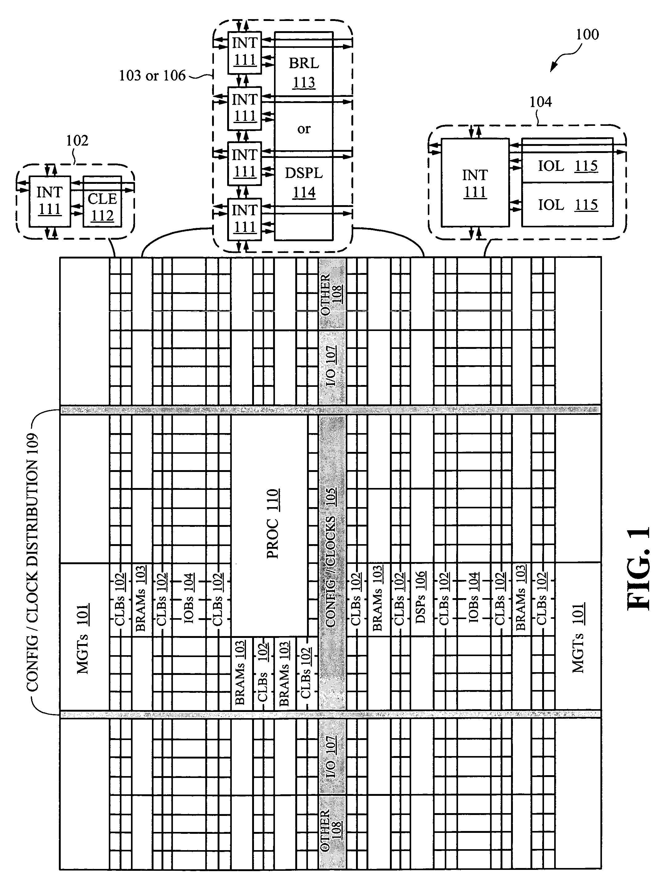
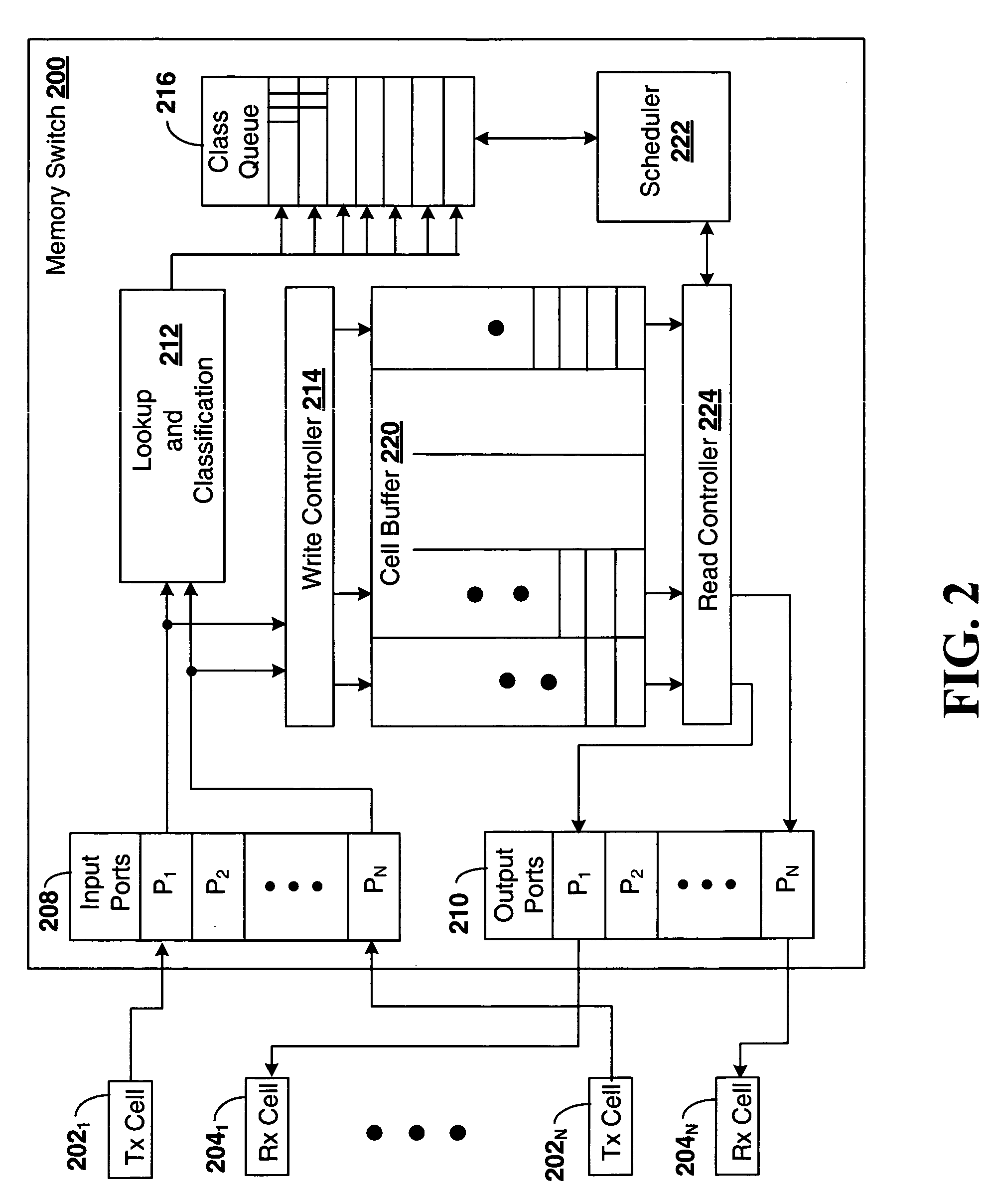
[0023]Embodiments of the present invention are described for use in an FPGA. The network switch according to the present invention provides for communications between nodes or modules programmed into the logic of an FPGA. The network switch is also programmed into the logic. Further, the FPGA memory can be configured to meet the parameters defined for the switch. Although the following description of embodiments of the present invention are described with respect to particular components of an FPGA, it is understood that other integrated circuits with on board programmable logic and memory can be programmed to include a network switch according to embodiments of the present invention. For reference, FIG. 1 shows one configuration of components of an FPGA that can be configured to include a network switch according to the present invention.

FPGA Overview

[0024]The FPGA of FIG. 1 includes a large number of different programmable tiles including MGTs 101, configurable logic blocks (CLBs ...


PUM


Abstract

A shared memory switch is provided for storing and retrieving data from BlockRAM (BRAM) memory of a PLD. A set of class queues maintain a group of pointers that show the location of the incoming “cells” or “packets” stored in the memory in the switch based on the time of storage in the BRAM. A non-blocking memory architecture is implemented that allows for a scalable N×N memory structure to be created (N=number of input and output ports). A write controller stripes the data across this N×N memory to prevent data collisions on read in or read out of data. The data is scheduled for read out of this N×N shared memory buffer based on priorities or classes in the class queues, with priorities being set by a user, and then data is read out from the BRAM.

Description

BACKGROUND[0001]1. Technical Field[0002]The present invention relates to a network switch providing communication between nodes that uses a BlockRAM (BRAM) memory of a Field Programmable Gate Array (FPGA) to store data.[0003]2. Related Art[0004]Traditional switching functions in network systems require the interconnection of various nodes, or modules that perform a specific function. Nodes can be formed on a single device, such as an Application Specific Integrated Circuit (ASIC), or multiple chips, with the nodes configured to communicate with one another. Communications are accomplished using direct communication links between the nodes over a circuit switched crossbar, or by using a bus structure.[0005]The crossbar switch provides a set of connecting wires, with no support for the data formats that are transmitted between nodes or modules formed in the logic. The crossbar connection scheme while providing extremely low latency for traversal times between the nodes provides no sup...

Claims


Application Information

Patent Timeline
IPC IPC(8): G06F7/38H03K19/173
CPCH03K19/177
Inventor KAVIPURAPU, GAUTAM NAGRAO, SWEATHAALTHOUSE, CHRIS
Owner XILINX INC
Why Eureka
Try Eureka