
Spatial light modulator with four transistor electrode driver

a technology of electrode drivers and transistors, applied in logic circuits, digital storage, instruments, etc., can solve the problems of increasing the silicon real estate used to fabricate arrays, the geometry of conventional sram cells restricts their applicability, and the number of transistors utilized, so as to reduce the size of electrode drivers, reduce the effect of real estate and faster write operations

Active Publication Date: 2008-10-28
MIRADIA INC
View PDF4 Cites 0 Cited by
  • Summary
  • Abstract
  • Description
  • Claims
  • Application Information

AI Technical Summary

Benefits of technology

"The present invention provides techniques for controlling mirrors in spatial light modulators, such as those used in display applications. The invention provides faster write operations and smaller electrode drivers compared to conventional techniques. The invention also utilizes minimum design rule transistors and reduces real estate usage. These technical effects provide improved performance and efficiency of spatial light modulators."

Problems solved by technology

However, DRAM cells leak charge during operation, resulting in the need to recharge the DRAM cells to the appropriate electrode voltage on a periodic basis.
SRAM cells are not susceptible to the current leakage problems characteristic of DRAM cells, but the number of transistors utilized and the geometry of conventional SRAM cells limit their applicability as the micro-mirror geometries decrease in size.
However, additional micro-mirrors of a conventional size increases the silicon real estate used to fabricate the array.
In some designs, the minimum design rules related to silicon processing of the SRAM cells limits the ability of a designer to reduce the size of the SRAM cells to support the fabrication of smaller micro-mirrors in high resolution display applications.

Method used


Image

  • Spatial light modulator with four transistor electrode driver
  • Spatial light modulator with four transistor electrode driver
  • Spatial light modulator with four transistor electrode driver

Examples


Embodiment Construction

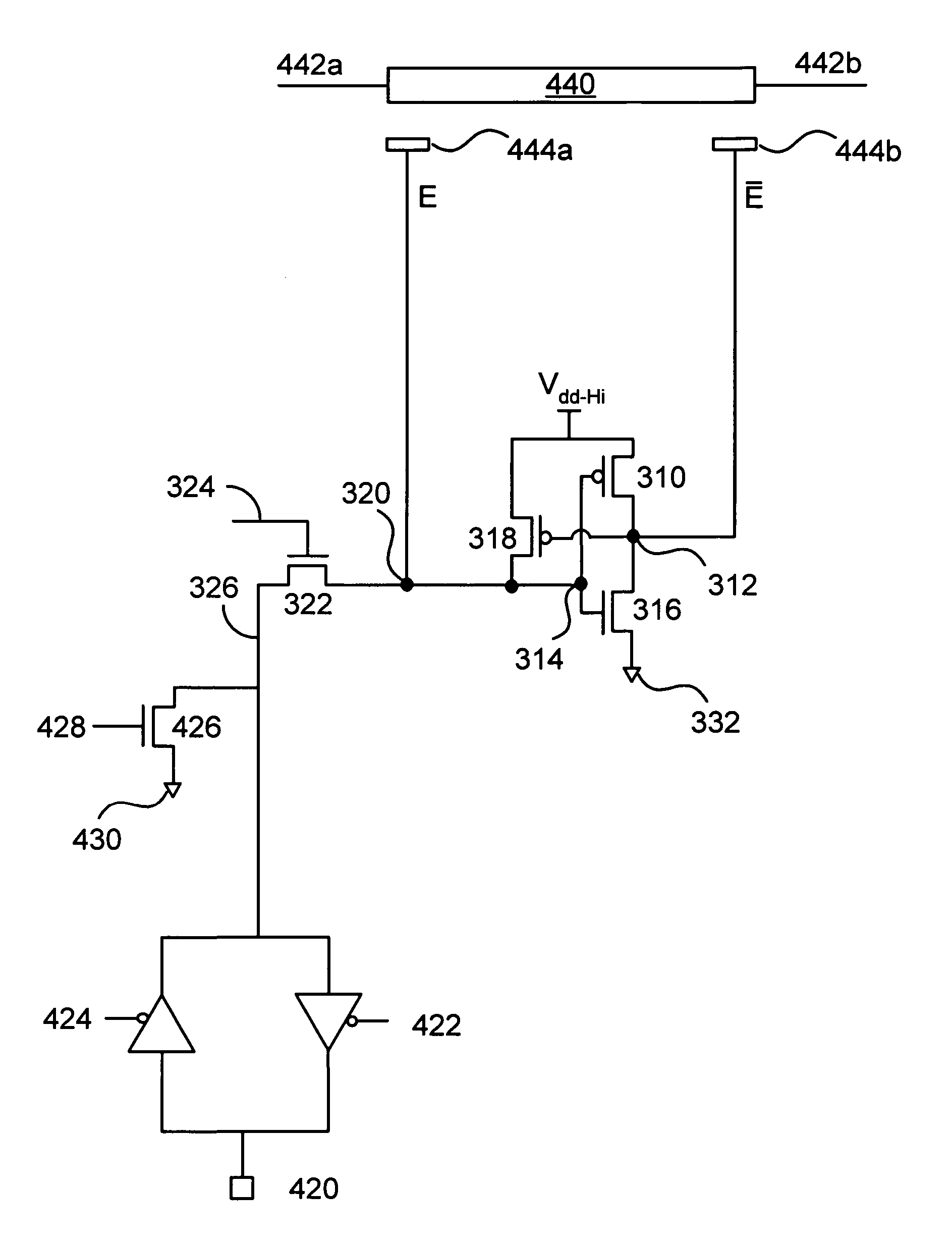
[0024]According to the present invention, techniques related to spatial light modulators are provided. More particularly, the invention relates to a method and apparatus for providing control circuitry for actuation of mirrors in a spatial light modulator. Merely by way of example, the invention has been applied to a design of addressing circuitry suitable for driving electrodes associated with micro-mirrors in a spatial light modulator used in a display application. The method and apparatus can be applied to spatial light modulators as well as other devices, for example, micro-electromechanical sensors, detectors, and displays.

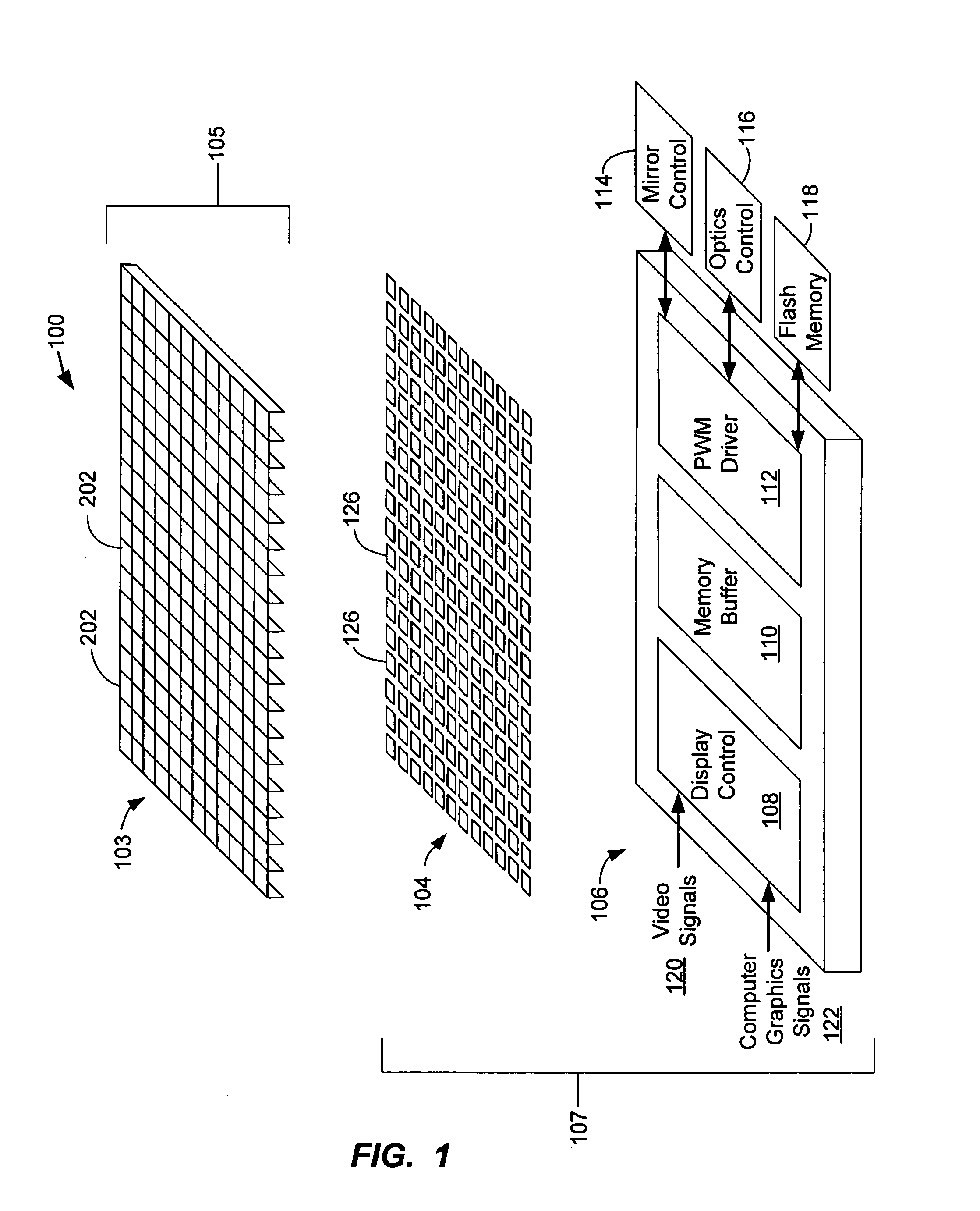
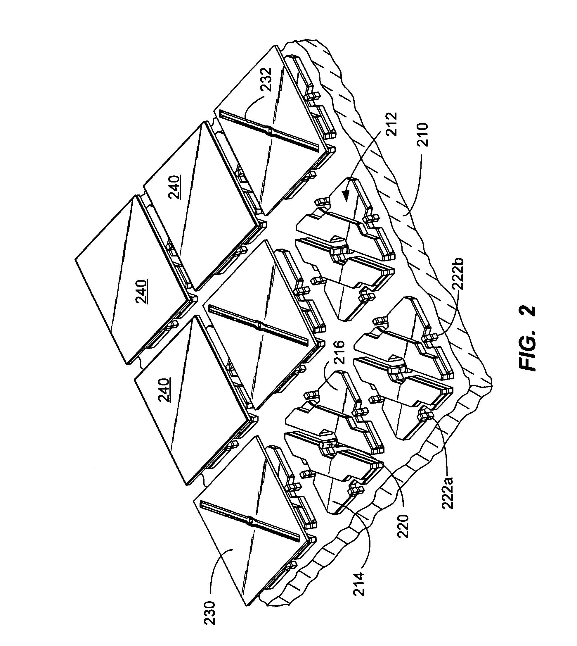
[0025]FIG. 1 is a diagram that illustrates the general architecture of a spatial light modulator (SLM) 100. The illustrated embodiment has three layers. The first layer is a mirror array 103 that has a plurality of deflectable micro-mirrors 202. In a preferred embodiment, the micro-mirror array 103 is fabricated from a first substrate 105 that is a single mat...


PUM


Abstract

A memory cell for driving a complementary pair of electrodes associated with a micro-mirror of a spatial light modulator. The memory cell includes a first PMOS transistor, wherein a source of the first PMOS transistor is coupled to a first supply voltage. The memory cell also includes a first NMOS transistor, wherein a drain of the first NMOS transistor is coupled to a drain of the first PMOS transistor, a source of the first NMOS transistor is coupled to a second supply voltage, and a gate of the first NMOS transistor is coupled to a gate of the first PMOS transistor. The memory cell further includes a second transistor adapted to establish a conduction path between the gate of the first NMOS transistor and at least one of the first supply voltage or the second supply voltage. Moreover, the memory includes a select transistor, wherein a drain of the select transistor is coupled to the gate of the first NMOS transistor and wherein the memory cell is free from a connection to a fifth transistor.

Description

BACKGROUND OF THE INVENTION[0001]This present invention relates generally to spatial light modulators. More particularly, the invention relates to a method and apparatus for providing control circuitry for actuation of mirrors in a spatial light modulator. Merely by way of example, the invention has been applied to a design of addressing circuitry suitable for driving electrodes associated with micro-mirrors in a spatial light modulator used in a display application. The method and apparatus can be applied to spatial light modulators as well as other devices, for example, micro-electromechanical sensors, detectors, and displays.[0002]Spatial light modulators (SLMs) have numerous applications in the areas of optical information processing, projection displays, video and graphics monitors, televisions, and electrophotographic printing. Reflective SLMs are devices that modulate incident light in a spatial pattern to reflect an image corresponding to an electrical or optical input. The ...

Claims


Application Information

Patent Timeline
Patent Type & Authority Patents(United States)
IPC IPC(8): G11C11/00
CPCG11C11/412
Inventor NGUYEN, THU
Owner MIRADIA INC
Learn More