Sensor semiconductor device and fabrication method of the sensor semiconductor device

a technology of semiconductor devices and fabrication methods, which is applied in the direction of photoelectric discharge tubes, instruments, electric discharge lamps, etc., can solve the problems of large increase in fabrication costs, circuit cracking and failure of electrical connections, and achieve cost-effective fabrication and improved reliability of subsequent fabrication processes

Active Publication Date: 2008-11-04
SILICONWARE PRECISION IND CO LTD
View PDF5 Cites 10 Cited by
  • Summary
  • Abstract
  • Description
  • Claims
  • Application Information

AI Technical Summary

Benefits of technology

[0007]In light of the foregoing drawbacks in the prior art, a primary objective of the present invention is to provide a low-cost sensor semiconductor device and a fabrication method thereof.
[0008]Another objective of the present invention is to provide a sensor semiconductor device and a fabrication method thereof, for preventing circuit cracking.
[0012]Therefore, by the sensor semiconductor device and the fabrication method thereof in the present invention, the sensor chip is firstly mounted on the substrate, and the sensor region of the sensor chip is covered with the transparent cover, and then the dielectric layer and the circuit layer are formed, wherein the circuit layer is electronically connected to the substrate and the sensor chip, and the transparent cover is exposed from the dielectric layer, such that external light can pass through the transparent cover to reach the sensor chip and allow the sensor chip to operate. Further, the sensor chip is electrically connected to the substrate through the circuit layer and can further be electrically connected to an external device via the solder balls mounted on the second surface of the substrate. In the present invention, the sensor chip can be tested and confirmed having normal functionality prior to being attached to the substrate, that is, only a sensor chip successfully passing the test is to be mounted on the substrate, such that the reliability of subsequent fabrication processes is improved and the known good die problem of the prior art can be solved. As the sensor chip is electrically connected to the substrate through the circuit layer and further electrically connected to the external device via the solder balls formed on the substrate, the circuit cracking problem of the prior art due to stress concentration can be avoided. Thus, the sensor semiconductor device of the present invention is cost-effectively fabricated.

Problems solved by technology

However, in the foregoing semiconductor device, a contact position between the circuit layer on the sidewall of the inclined opening and the electrode pad of the sensor chip forms an acute angle, making stress easily concentrated on the contact position and thereby leading to circuit cracking and failure in electrical connection.
Moreover, the semiconductor device is fabricated in the wafer stage, such that fabrication processes are complicated and the problem of known good die (KGD) cannot be effectively solved, thereby resulting in a great increase in the fabrication cost.

Method used


Image

  • Sensor semiconductor device and fabrication method of the sensor semiconductor device
  • Sensor semiconductor device and fabrication method of the sensor semiconductor device
  • Sensor semiconductor device and fabrication method of the sensor semiconductor device

Examples


Embodiment Construction

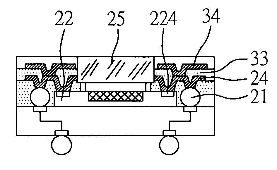
[0020]Preferred embodiments of a sensor semiconductor device and a fabrication method thereof proposed in the present invention are described as follows with reference to FIGS. 2 to 6. It should be noted that the drawings are simplified schematic diagrams only showing components relating to the present invention, and the arrangement of components could be more complex in practice.

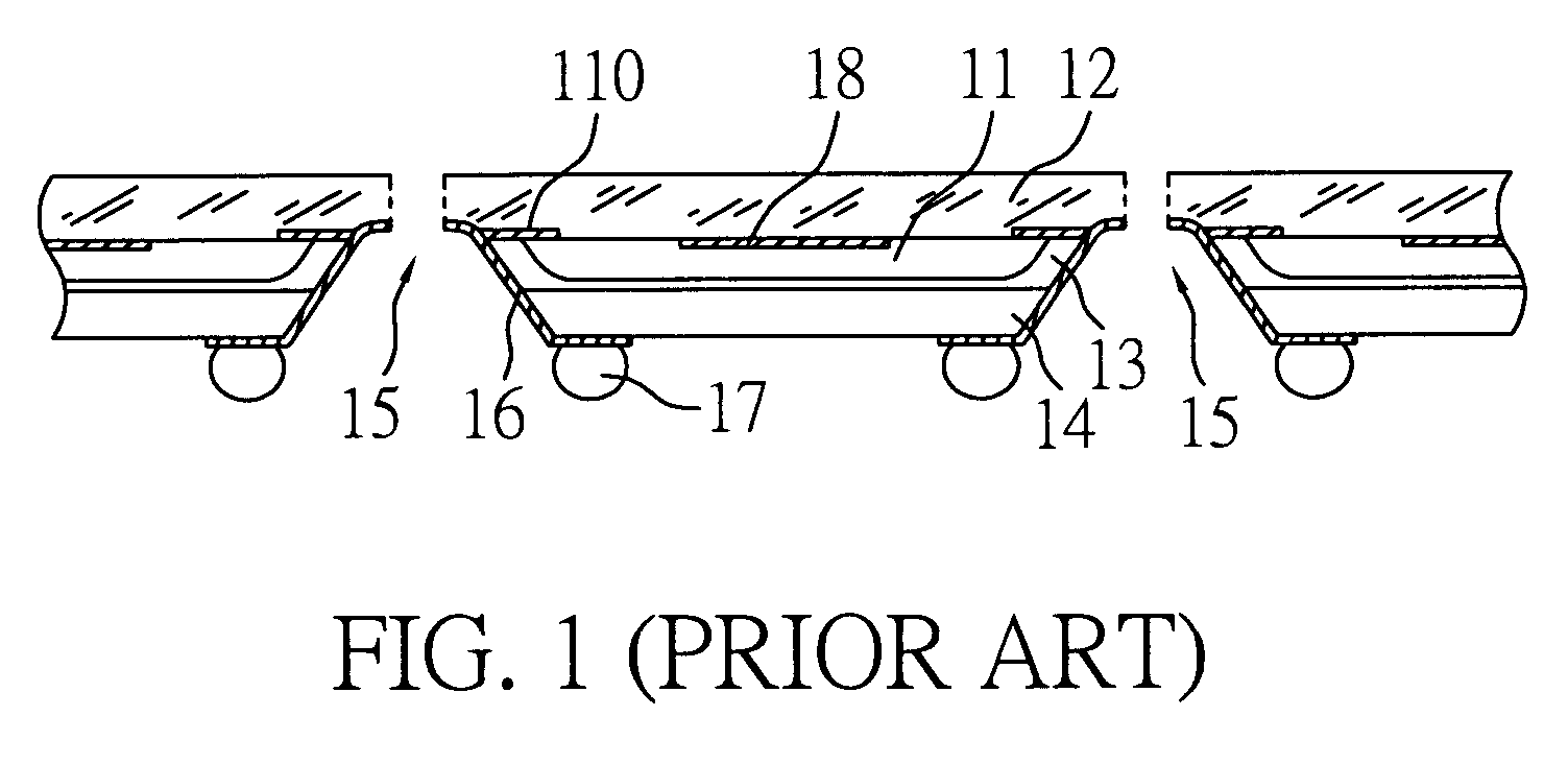
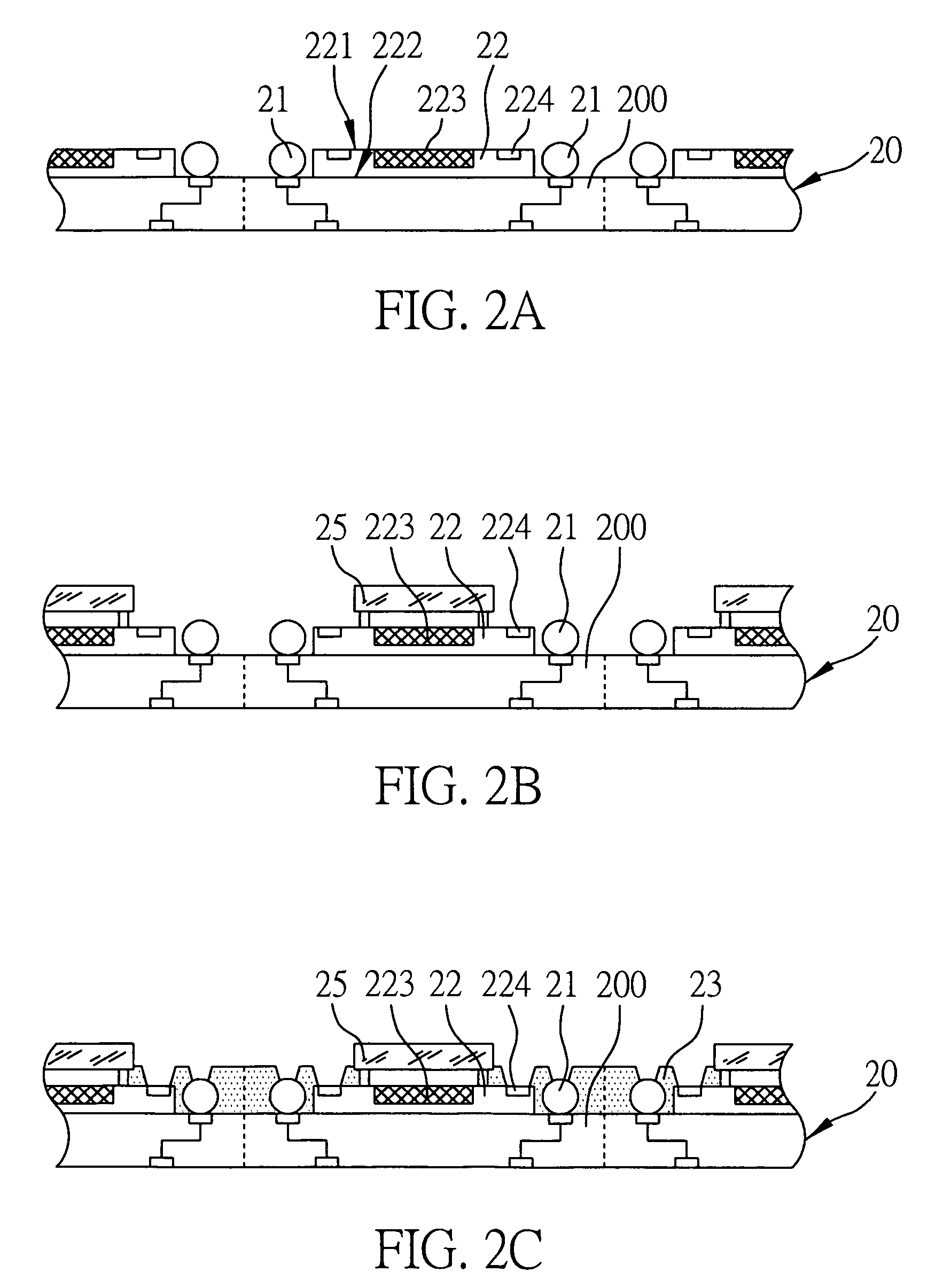
[0021]FIGS. 2A-2F show the steps of a fabrication method of a sensor semiconductor device according to a first preferred embodiment of the present invention. The following description relates to a batch-type fabrication method. It should be understood that the sensor semiconductor device of the present invention can also be fabricated in a single-type manner under appropriate fabrication conditions.

[0022]As shown in FIG. 2A, a substrate module plate 20 comprising a plurality of substrates 200 is provided, wherein each of the substrates 200 has a first surface and an opposed second surface, and a plurality o...


PUM


Abstract

A sensor semiconductor device and a fabrication method thereof are provided. The fabrication method includes mounting a sensor chip on a surface of a substrate; forming a transparent cover on the sensor chip; forming a dielectric layer and a circuit layer on the substrate, wherein the sensor chip is electrically connected to the substrate through the circuit layer and the transparent cover is exposed from the dielectric layer such that light can pass through the transparent cover to reach a sensor region of the sensor chip and allow the sensor chip to operate; and implanting a plurality of solder balls on another surface of the substrate to electrically connect the sensor chip to an external device. The sensor semiconductor device can be cost-effectively fabricated, and the circuit cracking and known good die (KGD) problems of the prior art can be avoided.

Description

FIELD OF THE INVENTION[0001]The present invention relates to sensor semiconductor devices and fabrication methods thereof, and more particularly, to a CSP (chip scale package) sensor semiconductor device and a method for fabricating the semiconductor device.BACKGROUND OF THE INVENTION[0002]Conventional image sensor package includes a sensor chip mounted on a chip carrier and electrically connected to the chip carrier via bonding wires, and a transparent cover for covering the sensor chip to allow light to be captured by the sensor chip through the transparent cover. The image sensor package can be used in various electronic devices such as digital still camera (DSC), digital video camera (DV), optical mouse, mobile phone, fingerprint recognizer and the like.[0003]In order to effectively reduce the size of the image sensor package, the CSP (chip scale package) technology is employed to form a CSP sensor semiconductor device, which desirably has a size slightly larger than the sensor ...

Claims


Application Information

Patent Timeline
Patent Type & Authority Patents(United States)
IPC IPC(8): H01J5/02H01L23/48
CPCH01L27/14618H01L27/14632H01L27/14687H01L24/97H01L2224/24225H01L2224/97H01L2224/82
Inventor HUANG, CHIEN-PINGHUANG, CHIH-MINGCHANG, CHENG-YI
Owner SILICONWARE PRECISION IND CO LTD
Why Eureka
Try Eureka