CMOS image sensor and method for fabricating the same

a metal oxide semiconductor and image sensor technology, applied in the field of image sensors, can solve problems such as noise resistance reduction, and achieve the effect of high noise resistan

Active Publication Date: 2008-11-11
INTELLECTUAL VENTURES II
View PDF4 Cites 27 Cited by
  • Summary
  • Abstract
  • Description
  • Claims
  • Application Information

AI Technical Summary

Benefits of technology

[0010]It is, therefore, an object of the present invention to provide a complementary metal oxide semiconductor (CMOS) image sensor having a high resistance toward noise by increasing an electron hole pair generation rate of a photodiode, and a method for fabricating the same.

Problems solved by technology

Such characteristic results in a decreased resistance towards noise.

Method used


Image

  • CMOS image sensor and method for fabricating the same
  • CMOS image sensor and method for fabricating the same
  • CMOS image sensor and method for fabricating the same

Examples


Embodiment Construction

[0017]A complementary metal oxide semiconductor (CMOS) image sensor and a method for fabricating the same in accordance with exemplary embodiments of the present invention will be described in detail with reference to the accompanying drawings.

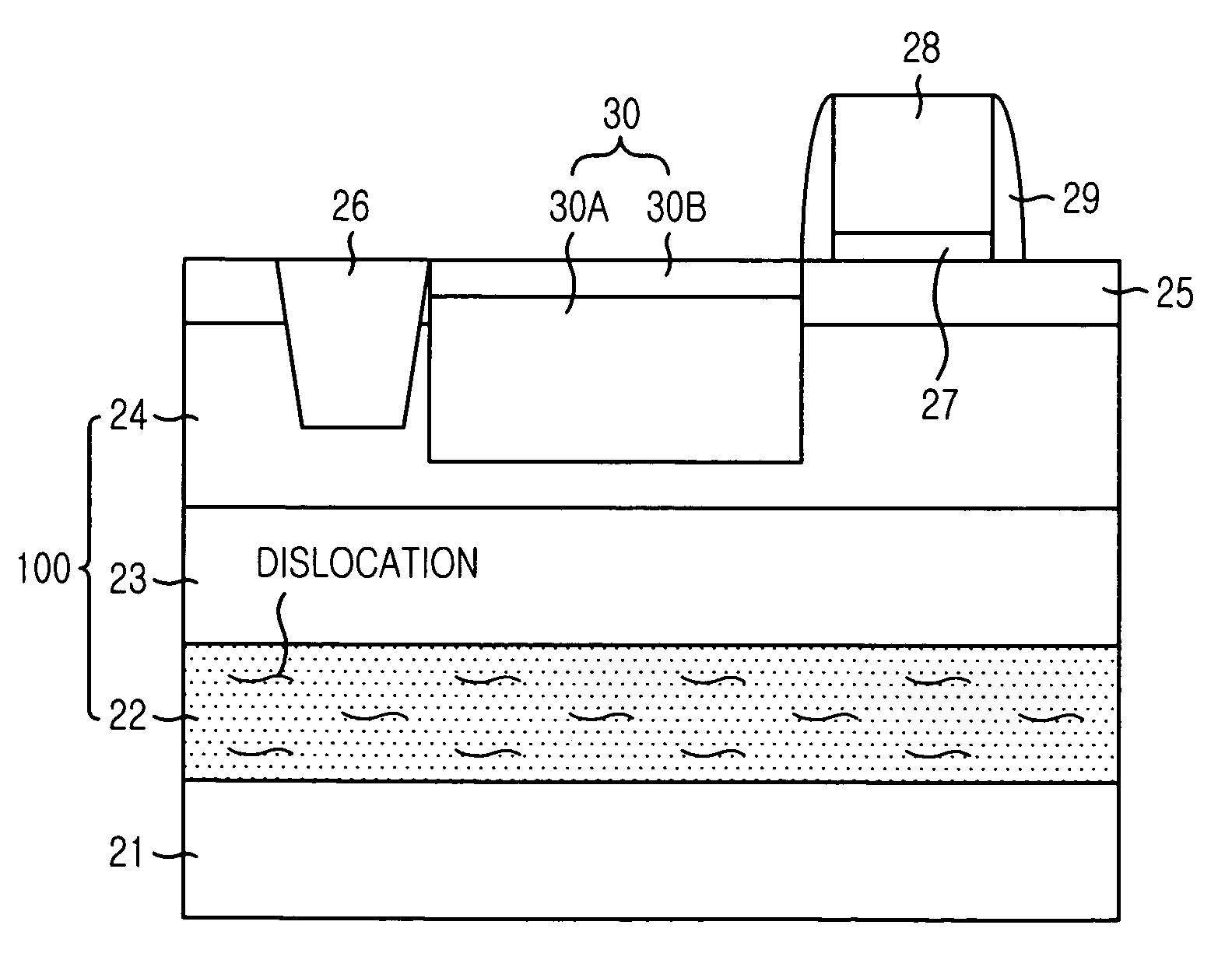
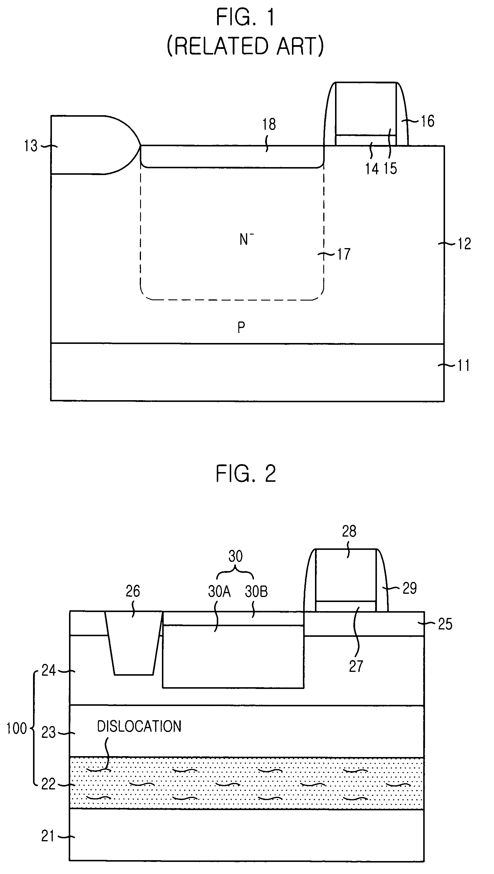
[0018]FIG. 2 is a cross-sectional view illustrating a CMOS image sensor in accordance with a specific embodiment of the present invention. A silicon germanium (SiGe) epitaxial layer 100 is formed over a substrate 21 including silicon. The SiGe epitaxial layer 100 is formed by an epitaxial growth process and is doped with a predetermined level of impurities, and the substrate 21 is doped with P-type impurities. An undoped silicon epitaxial layer 25 grown by employing an epitaxial growth process is formed over the SiGe epitaxial layer 100. A photodiode region 30 is formed from a top surface of the undoped silicon epitaxial layer 25 to a predetermined depth in the SiGe epitaxial layer 100. A gate pattern is formed over a predetermined portion of ...


PUM


Abstract

A CMOS image sensor includes a substrate including silicon, a silicon germanium (SiGe) epitaxial layer formed over the substrate, the SiGe epitaxial layer formed through epitaxial growth and doped with a predetermined concentration level of impurities, an undoped silicon epitaxial layer formed over the SiGe epitaxial layer by epitaxial growth, and a photodiode region formed from a top surface of the undoped silicon epitaxial layer to a predetermined depth in the SiGe epitaxial layer.

Description

FIELD OF THE INVENTION[0001]The present invention relates to an image sensor, and more particularly, to a complementary metal oxide semiconductor (CMOS) image sensor and a method for fabricating the same.DESCRIPTION OF RELATED ARTS[0002]Generally, an image sensor is a device that captures image information using a photo-reaction in a semiconductor material. The device transforms electrical values in pixels into a level capable of signalizing, each pixel detecting subjects with different brightness and wavelength. The image sensor generally includes a charge coupled device (CCD) image sensor and a complementary metal oxide semiconductor (CMOS) image sensor. The image sensor uses a photodiode as a photodetector, which absorbs light captured from an external subject image, and collects and accumulates photocharges.[0003]A typical unit pixel of a CMOS image sensor includes a photodiode and four transistors. The four transistors are a transfer transistor, which transfers photocharges int...

Claims


Application Information

Patent Timeline
Patent Type & Authority Patents(United States)
IPC IPC(8): H01L29/06H01L31/0328H01L31/0336H01L31/072H01L31/109H01L27/146
CPCH01L27/14601H01L27/14609H01L31/0352H01L27/14689H01L27/14643H01L27/146
Inventor CHA, HAN-SEOB
Owner INTELLECTUAL VENTURES II
Why Eureka
Try Eureka