Power semiconductor apparatus

a power semiconductor and case-type technology, applied in the direction of electrical apparatus construction details, solid-state devices, basic electric elements, etc., can solve the problems of parts and assembly costs that are higher than the industry standard, the case cannot be reused, and the productivity is inferior, so as to facilitate reuse of the case and improve the efficiency of the case. , the effect of excellent recyclability

Active Publication Date: 2008-11-11
MITSUBISHI ELECTRIC CORP
View PDF5 Cites 33 Cited by
  • Summary
  • Abstract
  • Description
  • Claims
  • Application Information

AI Technical Summary

Benefits of technology

[0009]The present invention has been implemented to solve the above described problems and it is an object of the present invention to provide a case type power semiconductor apparatus providing excellent productivity and excellent recyclability facilitating reuse of the case.
[0011]The present invention makes it possible to realize a case type power semiconductor apparatus providing excellent productivity and excellent recyclability facilitating reuse of the case.

Problems solved by technology

However, compared to the mold type IPM, the case type IPM includes more parts and requires higher assembly cost, and is therefore inferior in productivity.
Furthermore, as in the case of the mold type IPM, the case type IPM involves a problem that when the case is filled with resin, the case cannot be reused.

Method used


Image

  • Power semiconductor apparatus
  • Power semiconductor apparatus
  • Power semiconductor apparatus

Examples


first embodiment

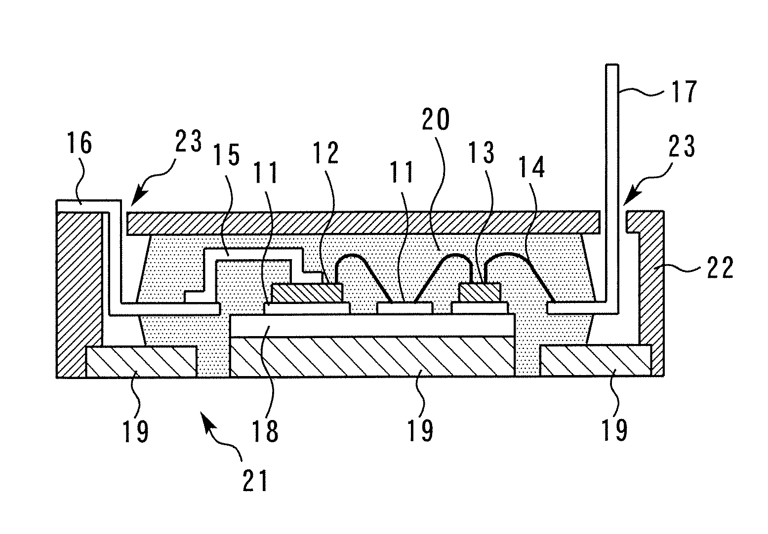
[0017]FIG. 1 is a sectional view showing a power semiconductor apparatus according to Embodiment 1 of the present invention. A power semiconductor element 12 such as an IGBT chip and diode and a control semiconductor element 13 such as a control IC are mounted on the main front surface of lead frames 11. These components are electrically connected to each other through Al wires 14. Furthermore, the power semiconductor element 12 is electrically connected to a power terminal 16 through a Cu terminal 15 and the control semiconductor element 13 is electrically connected to a control terminal 17 through an Al wire 14.

[0018]A heat sink 19 is provided through an insulation sheet 18 on the main back surface of the lead frame 11. A resin package 21 is formed by sealing these components with mold resin 20. Furthermore, the power terminal 16 and control terminal 17 are led out of the resin package 21. A part of the outside surface of the heat sink 19 is exposed from the resin package 21. The ...

embodiment 2

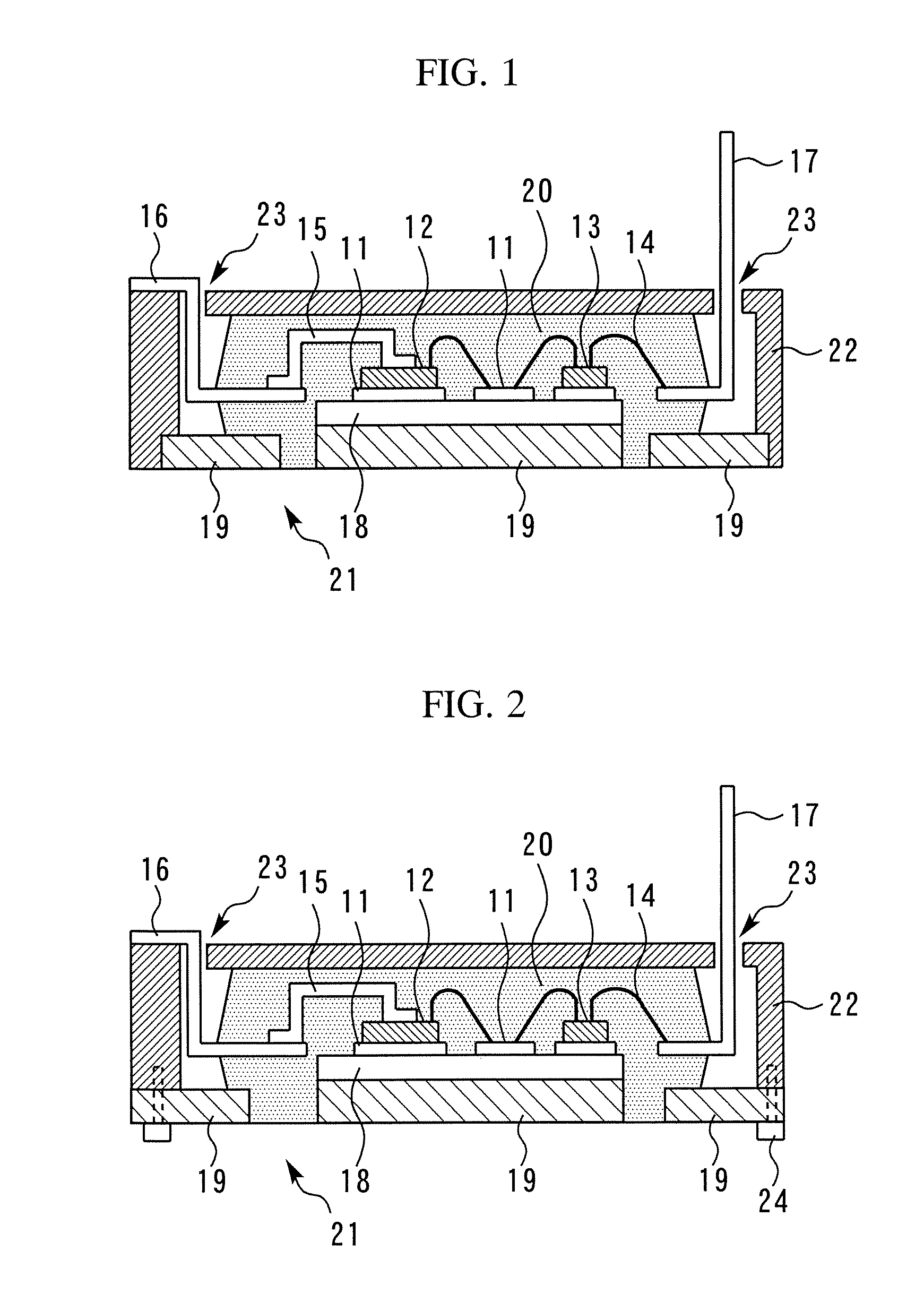
[0023]FIG. 2 is a sectional view showing a power semiconductor apparatus according to Embodiment 2 of the present invention. In this embodiment, peripheral edges of a heat sink 19 protrude from peripheral edges of an enclosure of a resin package 21 and are connected to open end edges of an insertion case 22 using bolts 24. The rest of the configuration is the same as that of Embodiment 1.

[0024]In this way, it is possible to reduce the number of parts and provide a power semiconductor apparatus with excellent assemblability, that is, excellent productivity. Furthermore, the strength of mounting the resin package and the case is greater than that of Embodiment 1.


PUM


Abstract

The power semiconductor apparatus includes a resin package made up of a power semiconductor element and a control semiconductor element which are mounted on a main front surface of a lead frame and sealed with mold resin, a power terminal led out of the resin package and electrically connected to the power semiconductor element, a control terminal led out of the resin package and electrically connected to the control semiconductor element and a cylindrical case which is formed in a manner separable from the resin package and encloses the resin package, wherein the power terminal and the control terminal are led out of lead insertion slots formed in the case, and a part of the power terminal which is led out of the case is bent along an end face of the case.

Description

BACKGROUND OF THE INVENTION[0001]1. Field of the Invention[0002]The present invention relates to a case type power semiconductor apparatus which encloses a power semiconductor element and a control semiconductor element with a case, and more particularly, to a power semiconductor apparatus providing excellent productivity and moreover excellent recyclability which facilitates reuse of the case.[0003]2. Background Art[0004]In recent years, there is a growing demand for IPM modularization of an IGBT module (Insulated Gate Bipolar Transistor) used for industrial motor control and servo applications. Here, “IPM” is a power module which incorporates a drive circuit and a self protection function for a power device such as a MOSFET and IGBT which controls power.[0005]A mold type IPM is used for consumer applications. This mold type IPM is made up of an IC and a power semiconductor chip (IGBT, diode) which are die-mounted on a Cu frame and consolidated with epoxy mold resin. There is also ...

Claims


Application Information

Patent Timeline
Patent Type & Authority Patents(United States)
IPC IPC(8): H01L31/0203
CPCH01L23/562H01L24/73H01L24/34H01L25/165H01L2924/1305H01L2924/1306H01L2224/73221H01L2224/45124H01L2924/01074H01L2924/01023H01L2924/01006H01L24/48H01L2224/48091H01L2224/48247H01L2924/01013H01L2924/01029H01L2924/01033H01L2924/01082H01L2924/13055H01L2924/13091H01L2924/19041H01L2924/00014H01L2924/00H01L2924/181H01L2224/40095H01L2224/40245H01L24/40H01L24/45H01L2924/14H01L2224/37147H01L24/37H01L2224/73265H01L2224/73263H01L2224/4826H01L2224/45099H01L2924/00012H01L2224/84H01L23/28H01L23/36
Inventor NAKANISHI, HIDETOSHISEKINE, TOSHITAKAOBARA, TAICHI
Owner MITSUBISHI ELECTRIC CORP
Why Eureka
Try Eureka