Dual work-function single gate stack

a single gate, work-function technology, applied in the direction of electrical apparatus, semiconductor/solid-state device manufacturing, semiconductor devices, etc., can solve the problems of cost and additional processing steps of the method used to form such devices, and achieve the effect of optimizing fet performan

Inactive Publication Date: 2008-11-11
ALSEPHINA INNOVATIONS INC
View PDF15 Cites 2 Cited by
  • Summary
  • Abstract
  • Description
  • Claims
  • Application Information

AI Technical Summary

Benefits of technology

[0013]Regardless of the embodiment of the method used to form the CMOS device, the first FET can be formed as an n-FET and the second FET can be formed as a p-FET. Alternatively, the first FET can be formed as a p-FET and the second FET can be formed as an n-FET. Selection of which FET comprise the p-FET and with comprises the n-FET depends upon the orientation of the semiconductor layer so as to optimize carrier mobility.

Problems solved by technology

While prior art CMOS devices have incorporated dual work-function gate electrodes as well as planar and non-planar FETs, the methods used to form such devices are costly, requiring a number of additional processing steps, including multiple gate masks.

Method used


Image

  • Dual work-function single gate stack
  • Dual work-function single gate stack
  • Dual work-function single gate stack

Examples


Embodiment Construction

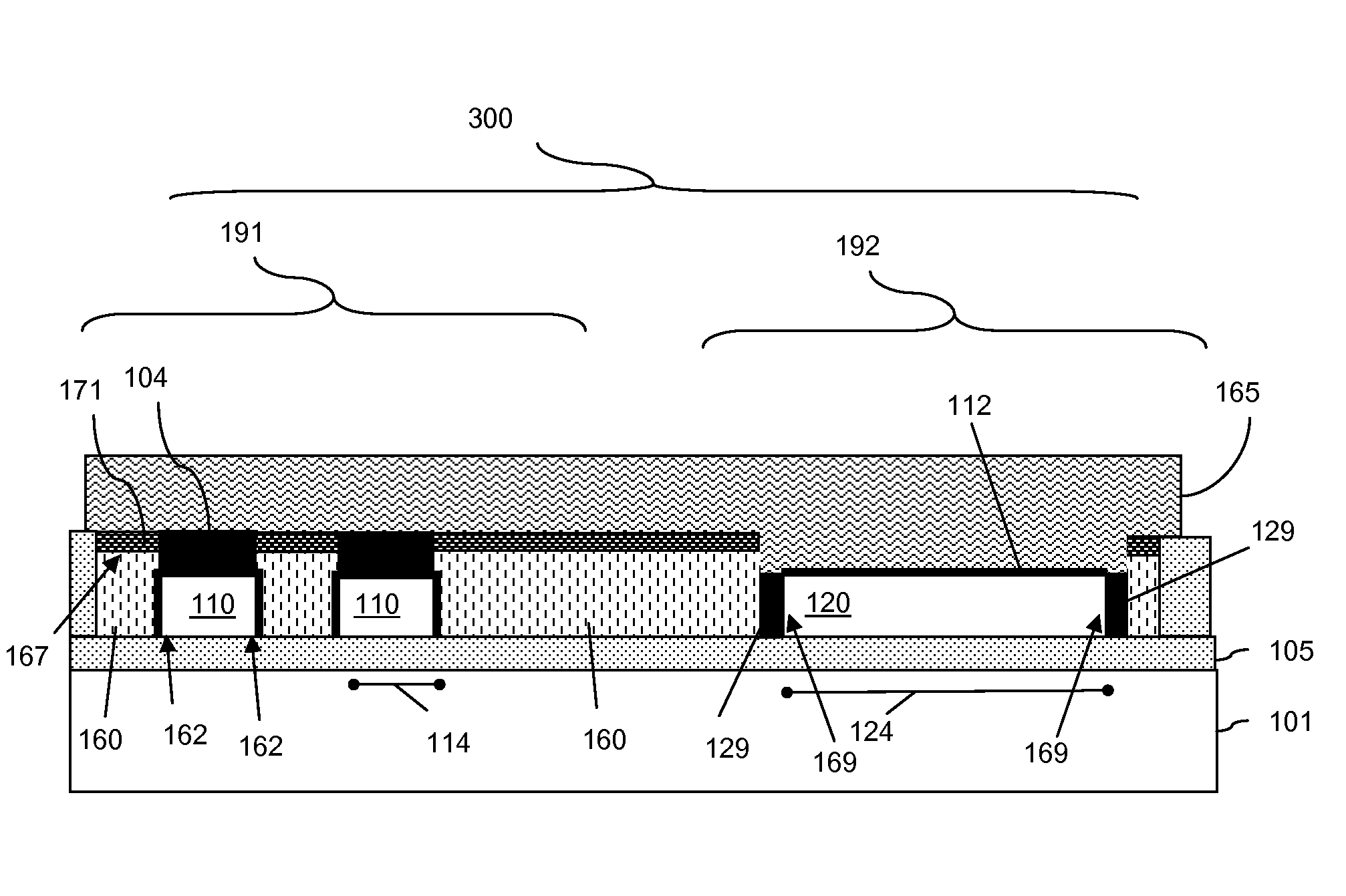
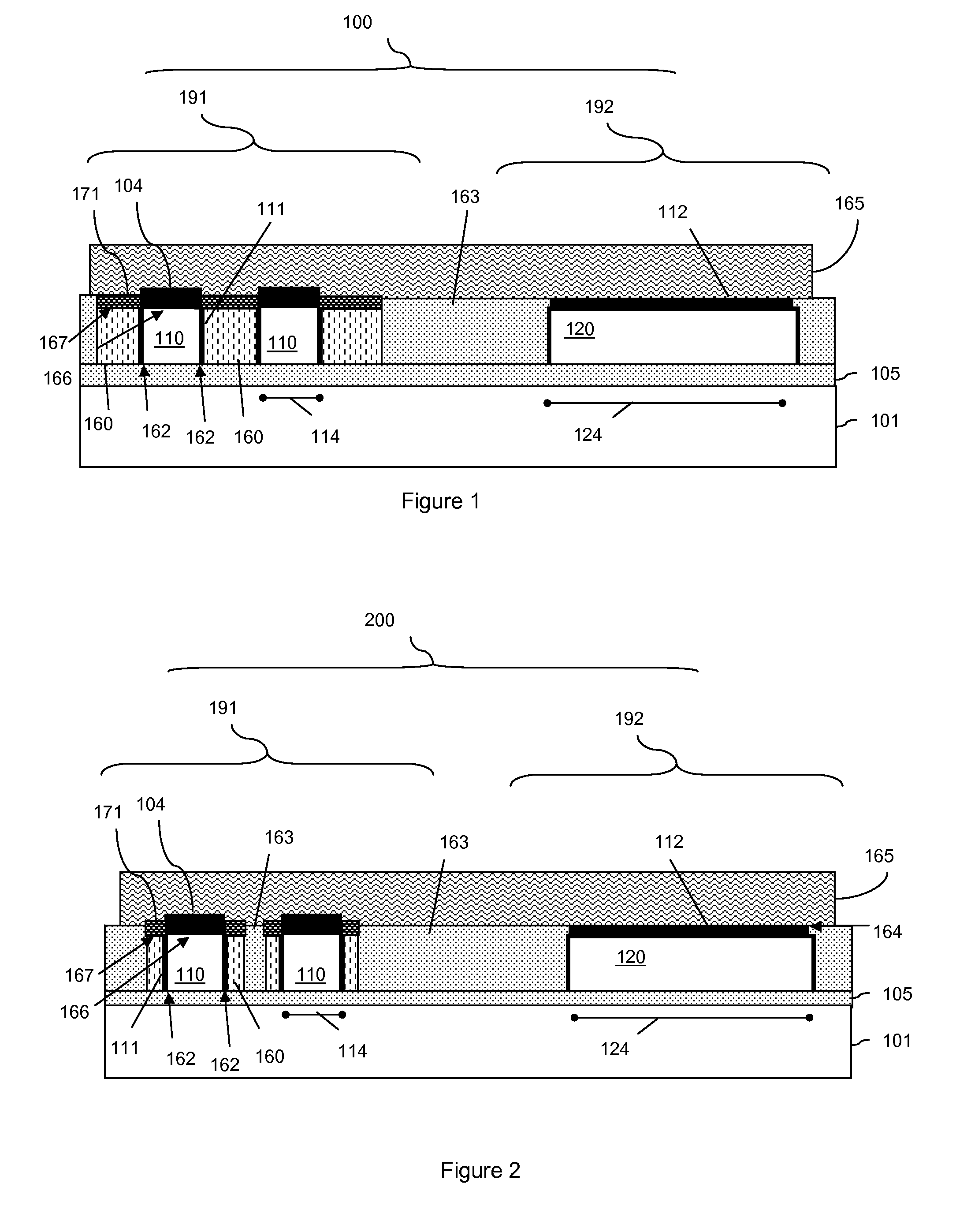
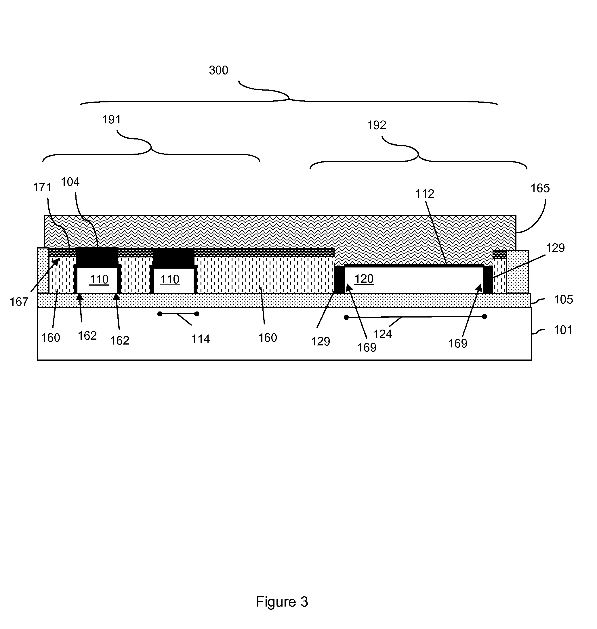
[0049]The embodiments of the invention and the various features and advantageous details thereof are explained more fully with reference to the non-limiting embodiments that are illustrated in the accompanying drawings and detailed in the following description. It should be noted that the features illustrated in the drawings are not necessarily drawn to scale. Descriptions of well-known components and processing techniques are omitted so as to not unnecessarily obscure the embodiments of the invention. The examples used herein are intended merely to facilitate an understanding of ways in which the embodiments of the invention may be practiced and to further enable those of skill in the art to practice the embodiments of the invention. Accordingly, the examples should not be construed as limiting the scope of the embodiments of the invention.

[0050]As mentioned above, while prior art complementary metal oxide semiconductor (CMOS) devices have incorporated dual work-function gate elect...


PUM


Abstract

Disclosed is a complementary CMOS device having a first FET with sidewall channels and a second FET with a planar channel. The first FET can be a p-FET and the second FET can be an n-FET or vice versa. The conductor used to form the gate electrodes of the different type FETs is different and is pre-selected to optimize performance. For example, a p-FET gate electrode material can have a work function near the valence band and an n-FET gate electrode material can have a work function near the conduction band. The first gate electrodes of the first FET are located adjacent to the sidewall channels and the second gate electrode of the second FET is located above the planar channel. However, the device structure is unique in that the second gate electrode extends laterally above the first FET and is electrically coupled to the first gate electrodes.

Description

BACKGROUND[0001]1. Field of the Invention[0002]The embodiments of the invention generally relate to dual work-function gate electrodes and, more particularly, to dual work-function gate electrodes on dual-plane high-mobility complementary metal oxide semiconductor devices.[0003]2. Description of the Related Art[0004]Recently, to enhance carrier mobility and, thus, performance of complementary metal oxide semiconductor (CMOS) devices, p-type field effect transistors (p-FETs) and n-type field effect transistors (n-FETs) have been formed on different planes within the same semiconductor layer. That is, to enhance performance CMOS devices have been formed that comprise different type devices: one with sidewall channels and one with a planar channel. Specifically, such a CMOS device can comprise a non-planar first type transistor (e.g., a p-FET) with a channel region that is perpendicular relative to the substrate (i.e., sidewall channels) so that it has a first orientation (e.g., a 110 ...

Claims


Application Information

Patent Timeline
Patent Type & Authority Patents(United States)
IPC IPC(8): H01L29/76H01L31/062H01L31/113H01L31/119
CPCH01L21/84H01L27/1203H01L21/823807H01L21/82385
Inventor ANDERSON, BRENT A.NOWAK, EDWARD J.
Owner ALSEPHINA INNOVATIONS INC
Why Eureka
Try Eureka